A couple of weeks ago, I blogged on GlobalFoundries’ silicon technologies supporting automotive radar applications. This time it is on GlobalFoundries’ silicon photonics technology which expects to find adoption in a broad spectrum of applications. The blog is based on listening to a technology presentation made by Dr. Anthony Yu, VP Computing and Wired Infrastructure, GlobalFoundries, Inc. at Linley’s Spring Processor Conference. His presentation was titled “Silicon Photonics Solutions Address Bandwidth, Reach, and Power Challenges” and is from a foundry’s perspective for enabling silicon photonics adoption on a large scale.
Silicon Photonics is the use of lasers for transferring data at high speeds among computer chips. In other words, it is optical I/O for rapid transmission of data. As a technology, it has been around for quite some time. But it hasn’t gained mass adoption yet. Does that mean it will remain so forever? Or is it in waiting for the right time and killer applications to get popularized? History tells us never to write off promising technologies.
Some technologies that are ubiquitous today had rough starts. It may be hard to believe that the now pervasive blue tooth technology had a few hiccups before it found widespread use. And so did the venerable USB technology. It is ironic that USB was initially popularized by Apple. Remember that Apple was pushing a competing technology in the form of FireWire. But the success of iMac that included USB ports set the course for rapid broad adoption of USB.
And who can forget the famous tagline, “The Network is the Computer” coined back in the mid-1980s. That was a time when networking communications was at a nascent stage. Cisco was in its infancy. But Sun Microsystems recognized that networking was the future of computing and coined this tagline. And made strategic decisions accordingly. They took the risk of incorporating SerDes technology in their workstation ASICs for implementing high speed I/O. Their competitor Silicon Graphics took a different route, at least in the earlier days by going broad on their chip I/Os. They soon ran into I/O bound chips that made the die larger than needed. They solved this issue by adopting flip-chip technology. Both SerDes technology and Flip-chip technology were not new at that time but needed the boost from some companies/products to proliferate into broad and rapid adoption across the industry.
Of late, due to a number of factors, silicon photonics solutions seem closer to wide adoption than ever before. The factors being, slowing down of Moore’s law, rapid increase in chip development costs, reduced die yield rates in very advanced process nodes, etc., This is pushing chiplets-based implementation as an alternative to monolithic system-on-a-chip (SoC) necessitating lots of high-speed connectivity between the different chiplets that make up the system. Silicon photonics may be one way to implement these interconnects.
Applications and Trends Pushing Silicon Photonics Toward Broader Adoption
Three major trends of frictionless networking, virtualization and hierarchical AI accelerated during the first twelve months of the covid pandemic period. The applications behind these trends appear to be the ones that are likely to tap into silicon photonics solutions (refer to Figure 1). There are three reasons to believe the adoption will happen soon.
- Heterogenous integration with optical interconnects becoming a serious alternative due to the fact that lithographic scaling is slowing down (Moore’s law slowing)
- Explosive growth of data (in zettabytes) due to proliferation of mobile applications
- Enormous consumption of electricity raising an existential threat flag. It is projected that if the growth of machine learning/artificial intelligence driven applications keeps up at the same rate as during the last year, they are expected to consume an amount equal to all electrical energy consumed today
Figure 1:
![]()
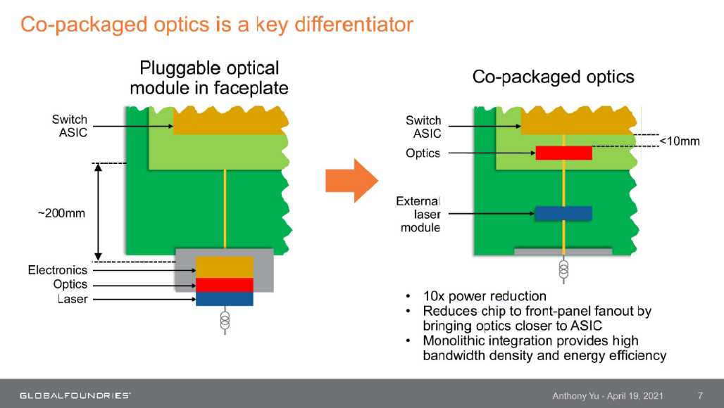
Markets that are currently being served by Silicon Photonics are the 100m to 10km data haul connectors of data centers, the 5G and the telecom markets. For the next wave of broader adoption, co-packaged optics is going to play a catalyzing role. Co-packaged optics means bringing the optics (which is typically in a face plate) very close to the ASIC (refer to Figure 2).
Figure 2:

GlobalFoundries’ Technology
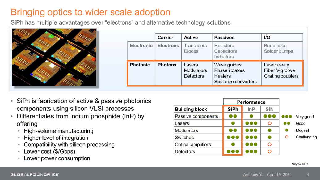
Historically, photonics industry has been working with hybrid silicon technologies such as indium phosphide. GlobalFoundries has established large scale CMOS-based foundry capacity to successfully manufacture photonics IC and optical components without special processing steps and additional associated costs. Although this approach is not a match for the indium phosphide approach, the benefits far outweigh the drawbacks (Refer Figure 3).
Figure 3:

In addition to offering the cost-effective manufacturability benefit, GlobalFoundries is offering some differentiating technologies for OSAT players to accelerate development of standardized packaging for implementing co-packaged optics. These are copper pillars, copper receive pads, on-die laser attach and v-groove based fiber attach technologies.
Summary
Dr. Yu’s presentation explored areas for broader adoption of Silicon Photonics through an approach of integrating complex CMOS and optical component functionality into a single photonic integrated circuit. If interested in benefitting from a silicon photonics solution, I recommend you register and listen to Dr. Yu’s entire talk and then discuss with GlobalFoundries on ways to leverage their different offerings for developing your products.
Also Read:
Enabling Silicon Technologies to Address Automotive Radar Trends and Requirements
Machine Learning Applied to Increase Fab Yield
Foundry Fantasy- Deja Vu or IDM 2?
Share this post via:


Solving the EDA tool fragmentation crisis