Machine learning applications have become pervasive and increasingly complex, from recommendation agents in online interactions to personal assistants for command response to (ultimately) autonomous vehicle control. Yet, an often overlooked facet of machine learning technology is the deployment in industrial process control systems.
The use of machine learning classification and decision algorithms can provide an immediate benefit in manufacturing yield (and thus, cost) and shipped product quality (through improved statistical variation control).
At the recent Advanced Semiconductor Manufacturing Conference (ASMC), sponsored by SEMI, Matthew McLaughlin from GLOBALFOUNDRIES provided an enlightening talk describing how the production fab team developed a machine learning method which resulted in significant yield improvements for a key, critical process flow step.[1]
We tend to focus on the recent advances in fabrication technology and equipment development that have enabled continued device and interconnect scaling. If I were to conduct a survey of SemiWiki readers, “What is the most critical step in microelectronics fabrication?” the answers would likely be dominated by newer technologies. High aspect ratio trench/contact etch. EUV lithography. Atomic layer deposition. In actuality, the most critical fab step has not changed in 50 years. The most important module in any fab is the photoresist spin coating system.
Photoresist Spin Coating
The figures below illustrate how photoresist is applied to the wafer, in preparation for mask layer lithography.
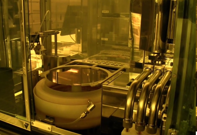
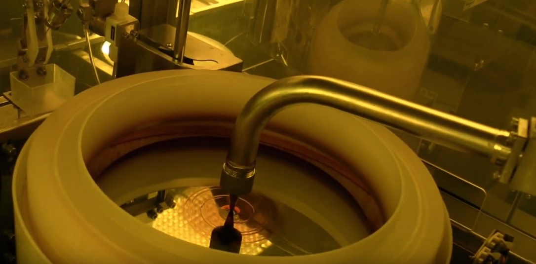
The wafer is mounted on a vacuum chuck. Photoresist is dispensed on the wafer surface, and a specific sequence of chuck spin ramp-up and steady-state RPM steps are used to distribute a thin uniform photoresist layer. (A preliminary step is also often employed – a solvent is applied to the wafer, which is spun and subsequently dried in N2 to pre-clean the surface and improve photoresist adhesion.) A special shroud around the chuck collects the excess photoresist which is centrifugally thrown off the wafer, to reduce any back-splash splatter.
The uniformity of the photoresist layer is absolutely critical. The subsequent lithography exposure step relies on the depth-of-focus and illumination dose to expose the photoresist, and ensure proper dimensions after developing the photoresist. And, of course, any material or particulate defects in the photoresist are local yield detractors.
The team at GLOBALFOUNDRIES focused on how to improve process control for the applied photoresist coat, inspected after the develop step.
Photoresist Layer Issues
There are several potential issues associated with the photoresist layer coat:
- “short” coverage (the wafer circumference is inadequately coated)
- “comet” streaking (often due to a surface contaminant)
- poor coverage at edges of the wafer
- “drip” issues (due to nozzle dispense irregularities)
- “splatter”
The photoresist dispensing nozzle may need cleaning or replacement, the spinner may need (preventive) maintenance, or a “bad batch” of photoresist may have been received from the chemical supplier. The emergence of an issue needs to be detected as quickly as possible – such as, during post-develop inspection – before any subsequent process steps. After the issue has been identified, and corrective actions taken, the photoresist layer can be readily stripped off and the coating step re-run, saving the work-in-progress (WIP) wafer lot.
Machine Learning and improved Photoresist Coating Defect Reduction
The difficulty associated with quality control inspection of the photoresist layer is that the thickness uniformity requirements are extremely stringent. For example, the image below highlights an area on the wafer that is out-of-spec, but imperceptible to visual inspection.
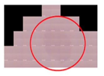
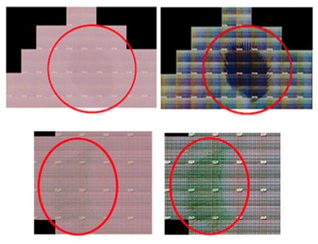
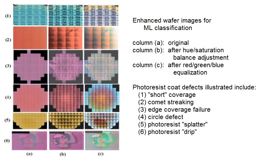
The GLOBALFOUNDRIES team pursued a machine learning approach to classification of the inspected wafer images. Due to the very slight local differences in image color/contrast, the images were first subjected to adaptations. Color hue + saturation balance adjustments were applied; subsequently, (strong) RGB equalization enhances the image contrast.
The figures below illustrate the result of these image processing steps – the top figure shows the enhanced image of the original wafer map above.
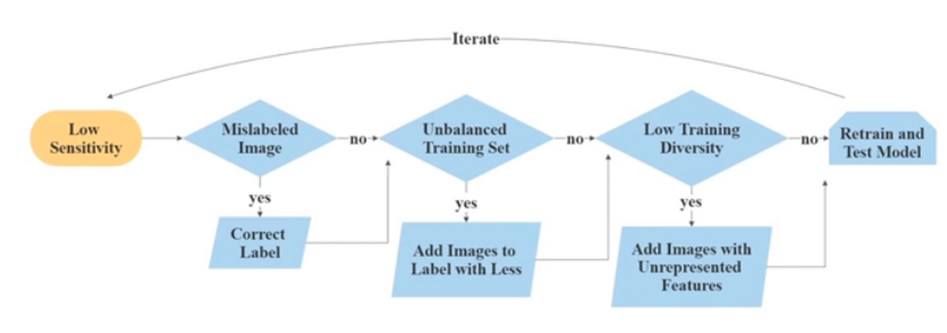
As with any machine learning model development, the GLOBALFOUNDRIES team prepared a (pre-classified) training and testing set of images, and refined the model to achieve a very high GOOD/BAD classification match result, as depicted in the flowchart below.
The figure below illustrates the various inspection issues, with enhanced image examples for each classification.
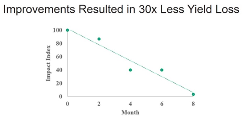
The figure below depicts the improvement in the “splatter” defect data, as this machine learning-based inspection model has been deployed in production – a 30X reduction in splatter photoresist defect impact. Wow.
As exemplified by this example at GLOBALFOUNDRIES, the application of machine learning technology to improve semiconductor fabrication process control offers considerable potential for yield and quality improvement.
-chipguy
References
[1] McLaughlin, M., et al., “Enhanced Defect Detection in After Develop Inspection with Machine Learning Disposition”, ASMC 2021, paper 8.1.
Also Read:
Foundry Fantasy- Deja Vu or IDM 2?
A Perfect Storm for GLOBALFOUNDRIES
Technology Optimization for Magnetoresistive RAM (STT-MRAM)
Share this post via:


Solving the EDA tool fragmentation crisis