You are currently viewing SemiWiki as a guest which gives you limited access to the site. To view blog comments and experience other SemiWiki features you must be a registered member. Registration is fast, simple, and absolutely free so please,
join our community today!
Machine learning applications have become pervasive and increasingly complex, from recommendation agents in online interactions to personal assistants for command response to (ultimately) autonomous vehicle control. Yet, an often overlooked facet of machine learning technology is the deployment in industrial process… Read More
In this article, we will explore the use of self-aligned litho-etch-litho-etch (SALELE) double patterning for BEOL metal layers in the 7nm node (40 nm minimum metal pitch [1]) with DUV, and 5nm node (28 nm minimum metal pitch [2]) with EUV. First, we mention the evidence that this technique is being used; Xilinx [3] disclosed the… Read More
State-of-the-art chips will always include some portions which are memory arrays, which also happen to be the densest portions of the chip. Arrayed features are the main targets for lithography evaluation, as the feature pitch is well-defined, and is directly linked to the cost scaling (more features per wafer) from generation… Read More
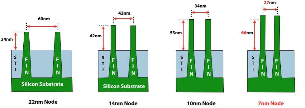
The use of hard masks instead of photoresist for the Extension implant is an effective way to optimize the amount of dopant that is retained along the fin sidewalls for those fins that border along photoresist edges (as discussed in Part 1 of this series).
However, hard masks do nothing to address the dominant problem driving steeper… Read More
At the SPIE Advanced Lithography Conference imec published a number of papers on EUV, multi-patterning and other lithography issues. In addition to seeing several of the papers presented I had a chance to sit down with imec’s director of advanced patterning, Greg McIntyre. In this article I will summarize my discussions… Read More
Irresistible Materials (IM) is a spin-out of the University of Birmingham in the United Kingdom that has been doing research on Photoresist and Spin-On Carbon hard masks for 10 years, most recently with Nano-C on chemistry development. IM has developed a unique EUV photoresist and they are now looking for partners to help bring… Read More
The annual SPIE Advanced Lithography Conference kicked off last night with vendor sponsored networking events and such. SPIE is the international society for optics and photonics but this year SPIE Advanced Lithography is all about the highly anticipated EUV technology. Scotten Jones and I are at SPIE so expect more detailed… Read More