WP_Term Object
(
    [term_id] => 14668
    [name] => Threshold Systems
    [slug] => threshold-systems
    [term_group] => 0
    [term_taxonomy_id] => 14668
    [taxonomy] => category
    [description] =>
    [parent] => 386
    [count] => 8
    [filter] => raw
    [cat_ID] => 14668
    [category_count] => 8
    [category_description] =>
    [cat_name] => Threshold Systems
    [category_nicename] => threshold-systems
    [category_parent] => 386
    [is_post] =>
)

WP_Term Object
(
    [term_id] => 14668
    [name] => Threshold Systems
    [slug] => threshold-systems
    [term_group] => 0
    [term_taxonomy_id] => 14668
    [taxonomy] => category
    [description] =>
    [parent] => 386
    [count] => 8
    [filter] => raw
    [cat_ID] => 14668
    [category_count] => 8
    [category_description] =>
    [cat_name] => Threshold Systems
    [category_nicename] => threshold-systems
    [category_parent] => 386
    [is_post] =>
)
Our friends at Threshold Systems have a new ONLINE class that may be of interest to you. It’s an updated version of the Advanced CMOS Technology class held last February. This is normally a classroom affair but to accommodate the recent COVID-19 travel restrictions it is being offered virtually.
As part of the previous class we did… Read More
Our friends at Threshold Systems have a new class that may be of interest to you. It’s an updated version of the Advanced CMOS Technology class held last May. As part of the previous class we did a five part series on The Evolution of the Extension Implant which you can see on the Threshold Systems SemiWiki landing page HERE. And… Read More
Part 4 of this series discussed how a transistor Extension could be fabricated in a planar device without using an implant operation, and is instead formed using a preferential etch followed by a selective epitaxial deposition. This final installment of the series will present the formation of an Extension in a FinFET transistor… Read More
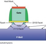
Perhaps the most innovative and effective Extension implant does not involve an implant at all, but is instead an etch followed by a selective epitaxial deposition.
In this Extension fabrication methodology the Source/Drains regions in a planar device are etched away in the normal fashion to accommodate the replacement Source/Drain… Read More
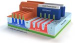
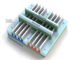
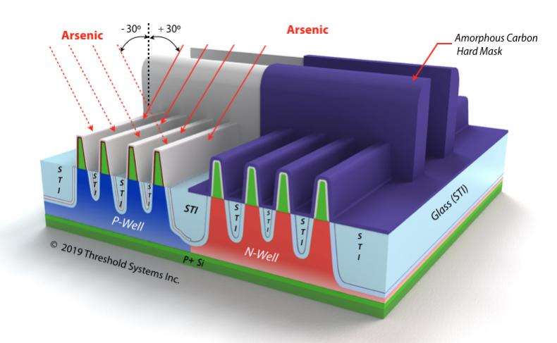
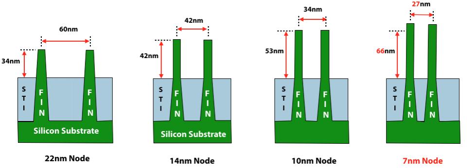
The problem of traditional FinFET Extension Implant doping concerns the awkward 3-dimensional structure of the fin. Because the Extension Implant defines the conductive electrical pathway between the Source/Drains and the undoped channel portion of the fin, it is essential that the fin be uniformly doped all three of its surfaces… Read More
The use of hard masks instead of photoresist for the Extension implant is an effective way to optimize the amount of dopant that is retained along the fin sidewalls for those fins that border along photoresist edges (as discussed in Part 1 of this series).
However, hard masks do nothing to address the dominant problem driving steeper… Read More
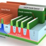
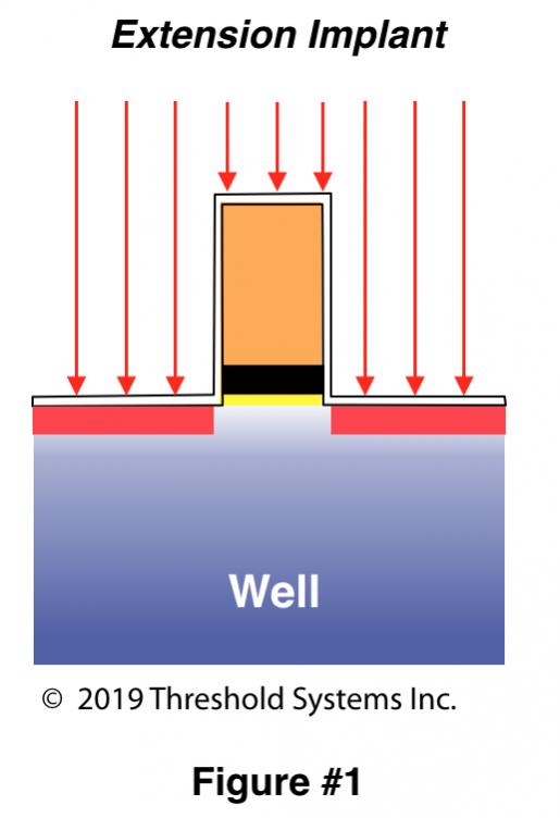
The 3D character of FinFET transistor structures pose a range of unique fabrication problems that can make it challenging to get these devices to yield. This is especially true for the all-important Extension implant that is put in place just prior to the nitride spacer formation.
The Extension implant is a central component of… Read More
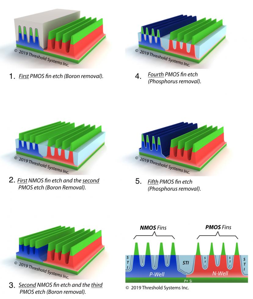
Like many others, we have often wondered why the PMOS fins on advanced microprocessors from Intel are narrower than the NMOS fins (6nm versus 8nm). This unusual dimensional difference first occurred at the 14nm node and it coincided with the introduction of Solid State Doping (SSD) of the fins at this node.
We have concluded that… Read More