In this article, we will explore the use of self-aligned litho-etch-litho-etch (SALELE) double patterning for BEOL metal layers in the 7nm node (40 nm minimum metal pitch [1]) with DUV, and 5nm node (28 nm minimum metal pitch [2]) with EUV. First, we mention the evidence that this technique is being used; Xilinx [3] disclosed the use of the technique in 7nm BEOL. Secondly, a minimum metal pitch as small as 28 nm leads to restricted illumination (low pupil fill) reducing the transmitted source power by 50% [4]. Throughput would be faster with the use of two EUV tools in series for double patterning (with 56 nm minimum metal pitch) since the number of wafers per day is tied to one litho tool handing off to the next. More seriously, stochastic defects [5] are a serious issue for single exposure at pitches ~30 nm [6]; however, pitch splitting by printing the same feature twice at twice the pitch exacerbates this [5]. Fortunately, SALELE [7] offers a way out, as will be explained below.
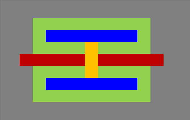
To achieve 14 nm features on a 28 nm pitch, for example, SALELE may start with 28 nm features, e.g., trenches, on a 56 nm pitch (Figure 1). This is advantageous over using 14 nm features on a 56 nm pitch or 28 nm pitch, due to the high incidence of EUV stochastic defects for the smaller features.
Figure 1. First patterned trenches (28 nm width on 56 nm pitch).
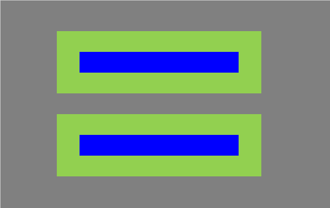
The trenches can be expanded, e.g., photoresist trimming [8], to 42 nm width. Then a 14 nm sidewall spacer is deposited and etched back to leave a 14 nm sidewall liner surrounding a 14 nm core feature filled within (Figure 2).
Figure 2. Trenches are expanded to 42 nm width, then sidewall liner of 14 nm formed on inside wall.
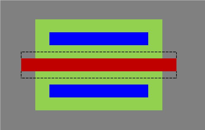
Outside and between two adjacent liners, an additional 14 nm trench may be patterned directly (actual width can be close to 28 nm); the liners help keep the latter trench aligned with the previous ones (hence, the self-aligned aspect) (Figure 3).
Figure 3. Additional trench patterned with alignment margin provided by the sidewall liners. The dotted line indicates the margin for printing or placing the feature.
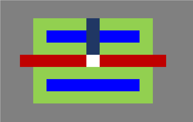
The trenches patterned at the two different stages can be filled with two different materials which etch differently, such as oxide and nitride. This allows those trenches to be cut more safely (Figure 4), since a cutting line can extend over the neighboring trench.
Figure 4. Trenches from the two stages are cut separately.
In total, four masks are used [7], two for the trenches, and two for the separate trench cuts. Self-aligned quadruple patterning (SAQP) using only DUV immersion tools can bring this down to three masks, but requires further process control maturity in addressing pitch walking [9].
While the cuts can be performed in EUV, they would suffer the previously mentioned stochastic defects issue, so DUV is more likely to be used. This would mean two EUV tools and two DUV tools being set up for the SALELE flow. This would be preferable to binding four EUV tools to this flow. For the earlier 7nm process [1], four immersion tools would be allocated. A more conventional self-aligned double patterning (SADP) can also reduce this to three masks, three tools. 20 nm features still pose a stochastic defect risk for EUV [5,6]. SALELE offers an easy transition from the LELE double patterning flow of the older 14/16/22nm nodes, but requires a substantial increase in lithography tooling.
References
[1] S-Y. Wu et al., “A 7nm CMOS platform technology featuring 4th generation FinFET transistors with a 0.027um2 high density 6-T SRAM cell for mobile SoC applications,” IEDM 2016.
[2] J. C. Liu et al., “A Reliability Enhanced 5nm CMOS Technology Featuring 5th Generation FinFET with Fully-Developed EUV and High Mobility Channel for Mobile SoC and High Performance Computing Application,” IEDM 2020.
[3] Q. Lin et al., “Improvement of SADP CD control in 7nm BEOL application,” Proc. SPIE 11327, 113270X (2020).
[4] D. Rio et al., “Extending 0.33 NA EUVL to 28 nm pitch using alternative mask and controlled aberrations,” Proc. SPIE 11609, 116090T (2021).
[5] P. de Bisschop and E. Hendrickx, “On the dependencies of the stochastic patterrning- failure cliffs in EUVL lithography,” Proc. SPIE 11323, 113230J (2020).
[6] J. Church et al., “Fundamental characterization of stochastic variation for improved single-expose extreme ultraviolet patterning at aggressive pitch,” J. Micro/Nanolith. MEMS MOEMS 19, 034001 (2020).
[7] Y. Drissi et al., “SALELE process from theory to fabrication,” Proc. SPIE 10962, 109620V (2019).
[8] L.Jang et al., “SADP for BEOL using chemical slimming with resist mandrel for beyond 22nm nodes,” Proc. SPIE 8325, 83250D (2012).
[9] H. Ren et al., “Advanced process control loop for SAQP pitch walk with combined lithography, deposition and etch actuators,” Proc. SPIE 11325, 1132523 (2020).
This article first appeared in LinkedIn Pulse: SALELE Double Patterning for 7nm and 5nm Nodes
Share this post via:





Is Intel About to Take Flight?