Spin-transfer torque magnetoresistive RAM (STT-MRAM) has emerged from several foundries as a very attractive IP option. An introduction to MRAM technology from GLOBALFOUNDRIES was provided in this earlier SemiWiki article. [1]
Briefly, STT-MRAM is a non-volatile storage option with the following attractive characteristics
- high storage duration
- high density (one access transistor connected to a magnetic tunnel junction)
- random access
- near-zero leakage power
- radiation-hard
- high-performance write cycle (with low write bit error rate)
There are limitations with STT-MRAM that require detailed process engineering:
- thermal sensitivity of the energy barrier that defines the spin-polarization stability (“the exchange stiffness”)
A key application area for embedded MRAM qualification is the automotive market, with its more demanding -40C to 150C temperature environment.
- limited endurance cycles
MRAM IP is targeted to displace embedded flash at more advanced process nodes – in this case, limited endurance is sufficient. For applications such as the last-level cache in high-performance SoCs, higher endurance is required.
The nature of the STT-MTJ requires unique modeling and micro-magnetic simulation techniques to optimize the selection of materials and physical dimensions. At the recent IEDM conference, GLOBALFOUNDRIES provided a perspective on the optimization of their MRAM technology offering. [2] This article summarizes their presentation.
Introduction
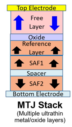
The magnetic tunnel junction (MTJ) consists of multiple ultrathin layers of unique metal and oxide materials, as illustrated in the figure below.
Recall that a material demonstrates magnetization due to the spin and orbit of its electrons.
A “soft” magnetic material only contributes to the magnetic flux around the material when an external magnetic field is applied – when the field is removed, there is no remnant magnetization.
A “hard” material is always magnetized. When an applied magnetic field in the opposite direction of the magnetization exceeds a critical value, the polarity of the magnetization reverses, and remains magnetized in this orientation when the applied field is removed. The magnetostatic energy in the hard material may differ based on the direction of the magnetization – i.e., a preferred direction in the absence of an external field – known as the magnetic anisotropy.
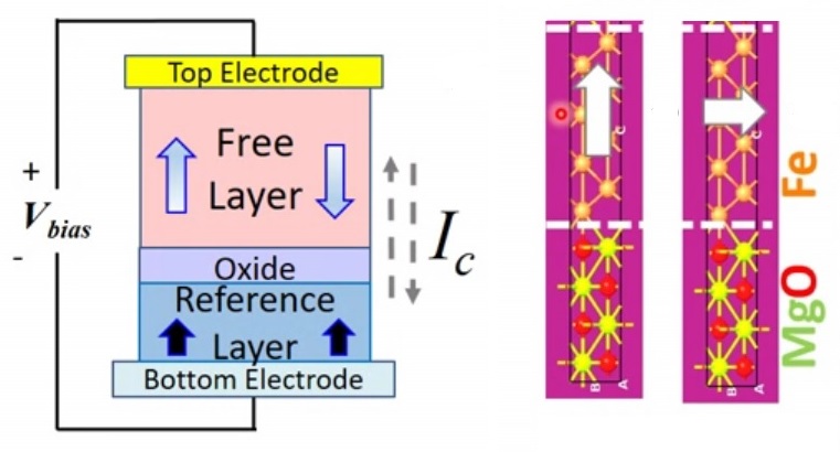
The configuration shown in the figure above is a perpendicular MTJ. The materials selected for the junction provide for a perpendicular magnetic anisotropy (PMA), which enables a stable, non-volatile “anti-parallel” magnetic state between the reference and free layers.
The figure below depicts the perpendicular TMJ interface between the magnetic layer and the oxide – note in the figure that an “in-plane magnetic anisotropy” device is also depicted, but does not contribute to the PMA.
The perpendicular MTJ is emerging as the preferred material stack, for the following characteristics:
- the PMA energy is larger for the p-MTJ than the in-plane anisotropy, with better retention at smaller MTJ sizes
- the critical current density through the MTJ area to switch the magnetization is less for the perpendicular junction
- as a result, the MRAM bitcell density may be much higher
The TMJ consists of a “reference” magnetic layer separated from a “free” magnetic layer by an extremely thin oxide. The free layer magnetization is switched between anti-parallel and parallel orientations to the reference layer, with a corresponding change in the junction electrical resistance (measured at low “read” current). The tunneling magnetoresistance ratio (TMR) achieved between the AP and P states is a key process development parameter, as it directly influences the memory read sense behavior.
The unique nature of the STT-MRAM cell is the manner in which the free layer magnetization is altered.
The angular momentum (“spin”) of an electron is normally random – thus, a conventional electrical current is non-polarized (1/2 spin-up, 1/2 spin-down).
However, an electron current through the reference layer produces a spin-polarized current through the tunnel oxide to the free layer. The angular momentum of this electron current can be transferred to the free layer electrons, due to “spin-transfer torque”. If the junction current magnitude is sufficient, the magnetic polarization of the free layer can be switched to parallel, as mentioned earlier for the case of an applied external magnetic field.
An electron current flowing in the opposite direction from the metal electrode re-orients the free layer magnetization to its anti-parallel orientation.
The first figure above also included “synthetic anti-ferromagnetic” (SAF) and metal spacer layers, as part of the MTJ stack. These additional layers help to increase the TMR ratio and improve the stability of the cell.
STT-MRAM DTCO
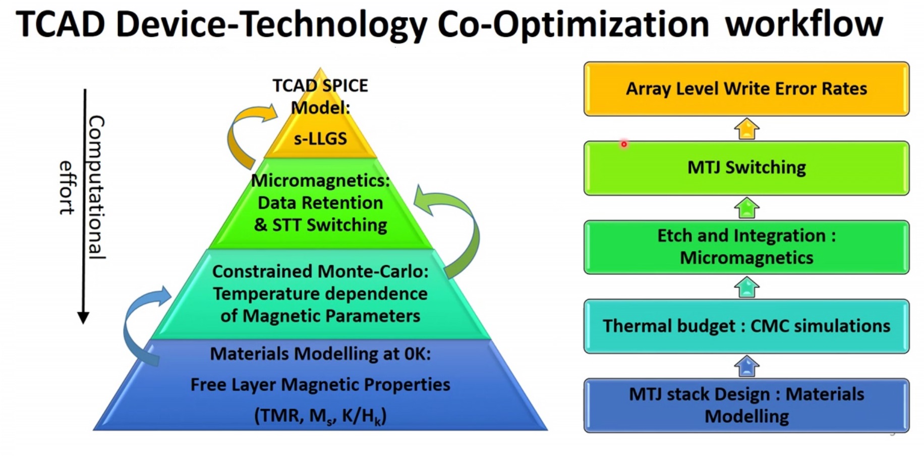
The GLOBALFOUNDRIES team provided an insightful view into STT-MRAM development, as summarized in the pyramid diagram above.
The first step (lowest pyramid level) in MRAM development is the stack engineering of materials – e.g., crystalline structure, atomic composition, thickness, and interface properties at each layer boundary. Detailed “spin-polarized” calculations are used to determine the follow material characteristics described earlier:
- magnetic anisotropy (K)
- magnetic saturation in the material (Ms)
- TMR
For example, the figure below illustrates a calculation of the “energy barrier” associated with the free layer interface to the neighboring oxide – as mentioned earlier, the perpendicular anisotropy is of interest (so the in-plane magnetization polarization energy is subtracted). The free layer in this example is a Cobalt-Iron (CoFe) material, roughly 10Angstroms thick; the tunnel oxide is MgO.
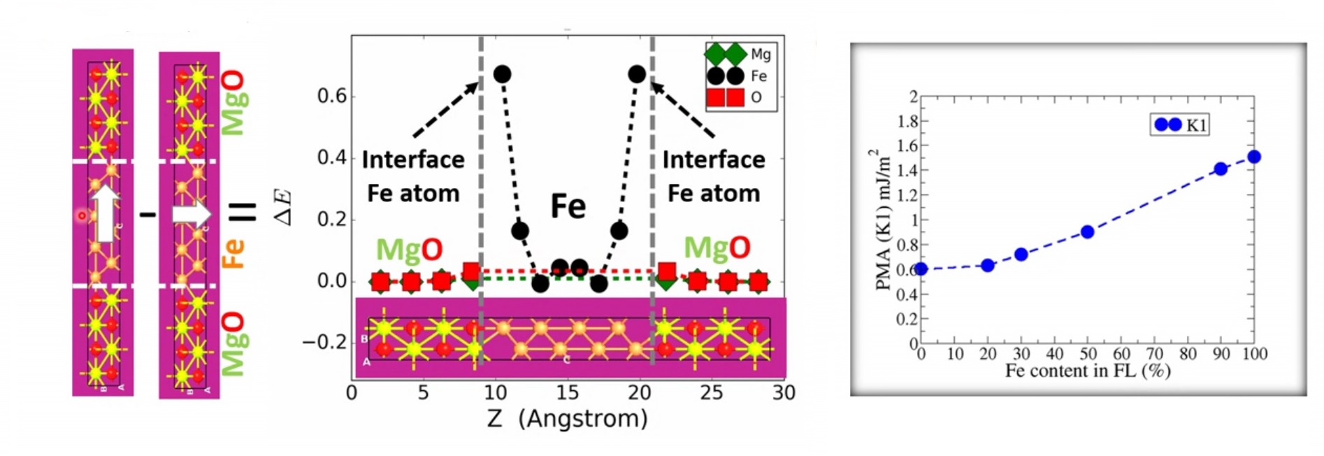
Recall from the discussion above that an increase in the PMA offers greater cell thermal stability and data retention – the adjoining figure above illustrates how this energy barrier changes based on the Co(x)Fe(1-x) material composition in the free layer.
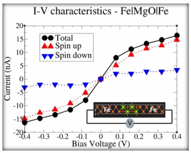
An additional material analysis relates to modeling the spin-polarized electron tunneling current through the MgO oxide layer, as illustrated below.
The next level of the DTCO pyramid is to extend these electron-level, “ground-state, zero K” material simulations to include the temperature dependence of: the material magnetic saturation (Ms); the magnetic anisotropy (K); and, the STT exchange behavior.
The figure below depicts how these properties change with temperature. The data enable process engineers to determine how the PMA stability energy barrier varies with temperature, and ultimately to define the bitcell write cycle current and duration requirements for the temperature range of interest.
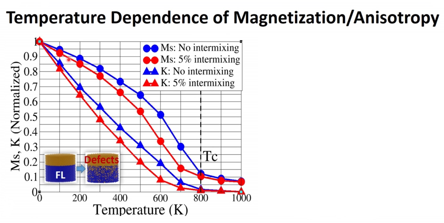
Note that the figure also includes an analysis of a “magnetic defect density” in the polarized material. During fabrication and assembly, a SoC containing an embedded MRAM will be subject to elevated annealing temperatures – e.g., a minimum of 260C for solder reflow. There will be some degree of non-magnetic layer atomic diffusion into the magnetic material.
The next level of the DTCO pyramid introduced the MTJ physical dimension into the process development. The figure below illustrates how magnetic “coupling fields” are present in a tapered, non-fully cylindrical MTJ after fabrication.

The figure above also depicts how the magnetic coupling field in the free layer is a function of the MTJ diameter and thickness. This external coupling introduces a dimensional asymmetry in the overall free layer-oxide interface, complicating the modeling of the parallel/anti-parallel switching behavior. A high field coupling at the periphery slows the write transition for either the P-to-AP or AP-to-P magnetization orientation. A detailed analysis is required to optimize the MTJ dimensions – large enough to avoid coupling-impacted write transition errors, yet still achieving array density and switching power targets.
The final, top level of the DTCO pyramid is the abstraction of the previous analyses of materials, temperature-dependence, and MTJ dimensional analysis into a suitable “compact device model” useful for MRAM array designers to incorporate with the SPICE models for array decode, bitcell access transistor, write driver, and read sense devices.
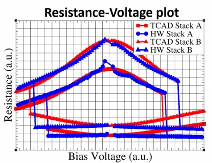
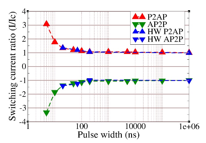
The success of the final compact model generation is depicted in the figures below. The first illustrates the (AP and P) DC resistance measured versus model for two different MTJ stack designs. The second figure depicts the interdependence between the required write pulse magnitude and duration, again showing excellent agreement between the compact model and measured MRAM hardware.
As highlighted above, the profile of the overall MTJ alters the coupling field to the switching free layer. The DTCO flow developed by GLOBALFOUNDRIES includes a statistical compact model, reflecting the process variation in the MTJ, and thus the coupling field.
The figure below illustrates the results of a Monte Carlo simulation analysis of the MRAM, using the compact model incorporating a statistical distribution of the coupling field. Again, excellent agreement with measured hardware is shown, when simulating the overall write error rate (“WER”), for a 20nsec write pulse width. (Note that when a short write pulse ends, there is a probabilistic measure that the free layer may “relax” back to its existing state, constituting a write error.)
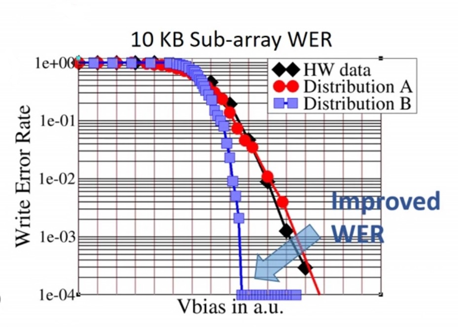
As an experiment, an artificial statistical distribution (“B”) for the MTJ profile and resulting coupling field was simulated, showing the strong dependence between MTJ process variation and WER. MRAM fabrication engineers are focused on improving the MTJ layer etch definition, to achieve better WER and correspondingly improved overall write cycle endurance.
Summary
GLOBALFOUNDRIES presented an extremely enlightening view into the complete DTCO flow for STT-MRAM development. Material characteristics are analyzed across (ground state and high-temp) conditions, resulting in input parameters used at higher levels of model abstraction. The influence of manufacturing variation – e.g., MTJ sidewall taper, material defect densities – were also incorporated into the overall model environment, due to the influence of coupling fields on MTJ behavior. The resulting compact models used in a traditional circuit design flow demonstrated excellent agreement with experimental hardware data.
I would encourage you to seek out a copy of the IEDM presentation from GLOBALFOUNDRIES to gain insights into the DTCO steps involved in MRAM process engineering.
-chipguy
References
[2] Dixit, H., et al, “TCAD Device Technology Co-Optimization Workflow for Manufacturable MRAM Technology”, IEDM 2020, paper 13.5.
Also Read:
3DIC Design, Implementation, and (especially) Test
Designing Smarter, not Smaller AI Chips with GLOBALFOUNDRIES
The Most Interesting CEO in Semiconductors!
Share this post via:


Solving the EDA tool fragmentation crisis