The introduction of direct die-to-die bonding technology into high volume production has the potential to substantially affect the evolution of the microelectronics industry. The concerns relative to the “end of Moore’s Law”, the diminishing returns of continued (monolithic) CMOS process scaling, and the disruptive effect of a transition from silicon to a more esoteric material could be deferred by the opportunity to develop extremely high volumetric density integration of silicon-based die (in heterogeneous process technologies).
There are challenges with 3DIC design, to be sure, from optimal system partitioning to (flexible) multi-die logical/physical database management to detailed thermal resistance analysis for the paths from internal die to package surface. yet, as more design examples emerge to illustrate how companies are addressing these challenges, the momentum for 3DIC adoption will certainly increase.
At the recent IEDM conference, GLOBALFOUNDRIES and Arm discussed an very interesting design test vehicle on which they had collaborated, using the 12nm FinFET and 3DIC bonding technology from GLOBALFOUNDRIES. [1] This article summarizes the highlights of that presentation.
The starting architecture for this design is shown in the figure below – specifically, note the Arm CoreLink CNM-600 mesh interconnect network used between cores.
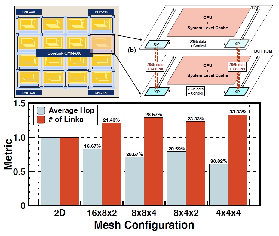
This network is a coherent mesh, optimized for Arm v8 generation processing elements; it is used to connect cores, accelerators, system cache, memory controllers, and I/O subsystems, and is extendible to multichip links. An Arm-based coherent mesh implies all processors/bus masters see the same “coherent” view of memory, through the cache and main memory hierarchy. Hardware-based coherency identifies shared resources between (small clusters of) cores, integrates cache snooping to identify if requisite data is already on-chip, and ensures appropriate write/read order propagation order.
This connection mesh offers an ideal partitioning boundary between die. The figure above illustrates the improvement in the number of mesh cross-point “hops” and the number of hardware links for various potential 3D configurations, compared to a planar implementation – a higher number of links across the 3D die enables fewer latency hops. For the 3DIC test vehicle, a 2×2 configuration of 4 mesh routers was implementation, as depicted in the figure.
The 3DIC bonding process flow at GLOBALFOUNDRIES is depicted in the figure below.
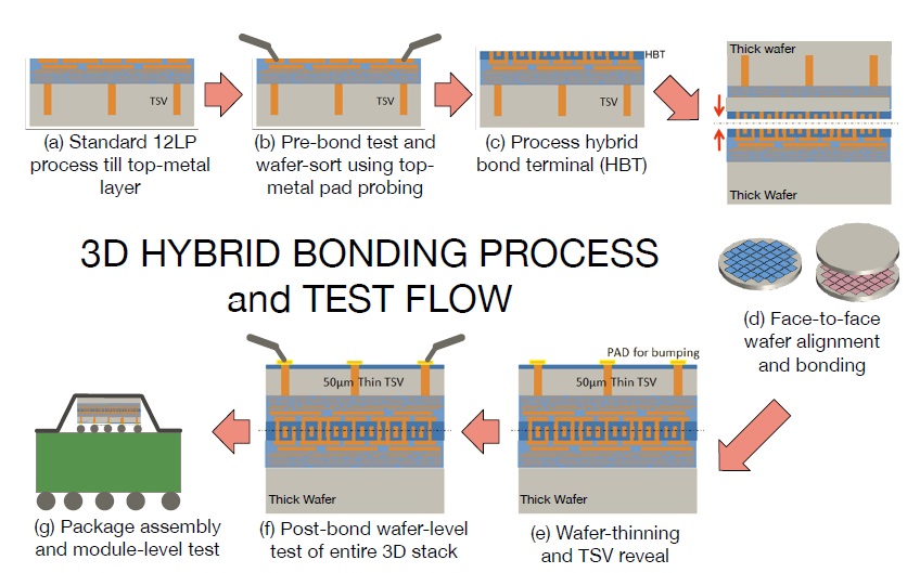
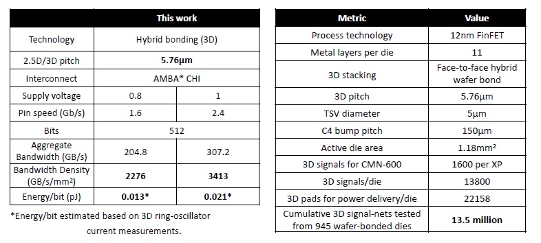
For this test vehicle, the pitch of the bond terminals is 5.76um, in a face-to-face die orientation. After addition of terminals, wafer alignment, and thermo-compression bonding, the top wafer is subsequently thinned to expose the through silicon vias (TSVs). Pads and bumps are added to the TSVs for final assembly and test.
A key implementation decision for any 3DIC design is the clocking and path timing analysis strategy. For this Arm/GLOBALFOUNDRIES vehicle, a fully-synchronous, single clock domain approach was selected – no synchronizing circuits were added at the die-to-die interface, and timing analysis required electrical data and path connectivity models that spanned the two die (in a single database). Specifically, the EDA placement methodology needed to “co-optimize” cell placement and bond locations across the die interfaces concurrently.
Testing
In addition to concurrent optimization of the physical implementation across die, 3DICs require early and thorough consideration of the design-for-testability (DFT) strategy. This entails:
- probe pad design and location decisions for wafer-level testing prior to bonding, to identify known good die (KGD)
The figure below provides a layout view of a die probe pad and die stack-to-package bump layout with the I/O cell.

- adding performance-measurement features to enable sorting KGD to align the timing distribution (for this synchronous, single clock domain design)
A separately adjustable VDD on each die can help tune out the process variation. A key 3DIC methodology decision relates to the static timing analysis design margins to allocation to the single domain 3D clock skew.
- integrating a cross-die DFT architecture to enable production (logical and electrical) testing of the hybrid bond interconnections
With the emergence of 3DIC assembly technology, the IEEE has recognized the need for a DFT standard, similar to the IEEE 1149 JTAG boundary scan definition. The 3DIC ARM/GLOBALFOUNDRIES test vehicle implements the IEEE 1838 DFT standard for 3DIC testing, as illustrated below. [2, 3]
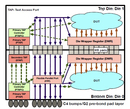
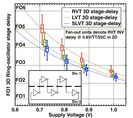
For this test vehicle, additional circuitry was included to characterize the electrical delay of (synchronous) timing paths that cross the die, as well as to test the fidelity of (a large number) of die-to-die bond connections. The figure below illustrates that the “3D inverter FO=1” delay is comparable to a 2D FO=3 gate delay (~20psec for 12nm FinFET), less at a higher voltage supply.
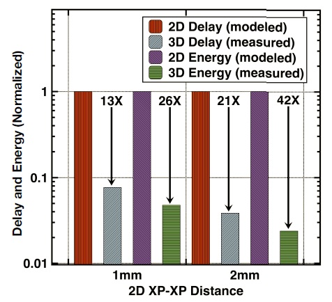
The partitioning of the Arm coherent mesh architecture into a 3DIC implementation enables vertical orientation of the cross-point router blocks. The figure below illustrates the link-to-link delay and power comparison between the 3D positioning versus a 2D lateral distance of ~1mm.
The electrical characteristics of bandwidth and power for this 3DIC test vehicle are summarized in the table below.
Summary
3DIC technology will offer attractive signal bandwidth and energy-per-bit interface communications, compared to multi-millimeter lateral interconnections on a monolithic die. An example test vehicle was recently presented by Arm and GLOBALFOUNDRIES, illustrating an ideal system partitioning for a 3DIC design – e.g., the cross-point links for a synchronous system design across the die-to-die interface.
The hybrid bonding technology from GLOBALFOUNDRIES was demonstrated to be highly manufacturable – characterization of the interconnect test chains across the die-to-die interface showed a low-variation resistance.
The 3DIC design methodology requires several unique considerations:
- employing a comprehensive, multi-die design database
- concurrent I/O, TSV, and bond pad assignment
- inter-die logic cell co-placement
- static timing analysis margin assumptions appropriate for inter-die paths
- performance measurement circuitry on-die (for KGD sort)
and, especially
- the (IEEE 1838) DFT architecture for the final 3DIC assembly
With the emerging IEEE standard and increasing EDA tool support, 3DIC design implementations will undoubtedly see greater adoption in the very near future.
-chipguy
References
[1] Sinha, S., et al, “A high-density logic-on-logic 3DIC design using face-to-face hybrid wafer-bonding on 12nm FinFET process”, IEDM 2020, paper 15.1.
[2] https://standards.ieee.org/standard/1838-2019.html
[3] https://ieeexplore.ieee.org/document/7519330
Also Read:
Designing Smarter, not Smaller AI Chips with GLOBALFOUNDRIES
The Most Interesting CEO in Semiconductors!
GLOBALFOUNDRIES Goes Virtual with 2020 Global Technology Conference Series!
Share this post via:


Is Intel About to Take Flight?