Keysight Technologies returns to 2026 DAC, The Chips to Systems Conference this year as a Silver Sponsor and an “I LOVE DAC” sponsor, bringing its Design Engineering Software portfolio to Booth #927 at DAC 2026, which runs July 26-29 in Long Beach, Calif. The Keysight team will be on-site Monday through Wednesday … Read More
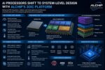
Artificial intelligence processors are entering a new era. For more than two decades, semiconductor innovation was driven primarily by transistor scaling and process node shrinks. Today, however, AI infrastructure demands are growing faster than traditional Moore’s Law improvements can sustain. The industry is now shifting… Read More
Dr. Dave Hwang joined Alchip in 2021 as General Manager of Alchip’s North America Business Unit. He also serves as Senior Vice President, Business Development. Prior to join Alchip, Dave served as Vice President, Worldwide Sales and Marketing for Global Unichip and in a variety of management and technical roles at TSMC.
Tell
…
Read More
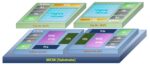
Today Alchip Technologies, a Taipei-based leader in high-performance and AI computing ASICs, announced a significant milestone with the successful tape-out of its 3D IC test chip. This achievement not only validates Alchip’s advanced 3D IC ecosystem but also positions the company as a frontrunner in the rapidly evolving field… Read More
Dan is joined by Dr. Julien Ryckaert who joined imec as a mixed-signal designer in 2000, specializing in RF transceivers, ultra-low power circuit techniques, and analog-to-digital converters. In 2010, he joined imec’s process technology division in charge of design enablement for 3DIC technology. Since 2013, he oversees… Read More
Dan is joined by Dr. John Ferguson, Director of Product Management for the Calibre nmDRC and 3DIC related products for Siemens EDA. John has worked extensively in the area of physical design verification. Holding several patents, he is also a frequent author in the physical design and verification domain. Current activities … Read More
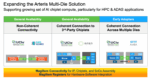
I am tracking the shift to multi-die design, so it’s good to see Arteris extend their NoC expertise, connecting chiplets across an interposer. After all, network connectivity needs don’t stop at the boundaries of chiplets. A multi-die package is at a logical level just a scaled-up SoC for which you still need traffic routing and… Read More
Alchip Technologies Ltd., a global leader in high-performance computing (HPC) and artificial intelligence (AI) ASIC design and production services, continues its trajectory of rapid growth and technical leadership by pushing the boundaries of advanced-node silicon, expanding its global design capabilities, and building… Read More
In this episode of the Semiconductor Insiders video series, Dan is once again joined by Anna Fontanelli, founder and CEO of MZ Technologies. In this discussion, more details of the challenges presented by advanced packaging and multi-die design are explored. Anna provides details of what’s involved in architectural … Read More