
At the recent VLSI Symposium on Technology and Circuits, Dr. Y.J. Mii, Senior Vice President of Research and Development at TSMC, gave a plenary talk entitled, “Semiconductor Innovations, from Device to System”. The presentation offered insights into TSMC’s future R&D initiatives, beyond the current roadmap. The associated… Read More

Author: Tom Dillinger
Future Semiconductor Technology Innovations
Clocking for High-Speed SerDes
The incessant demand for faster data rates across a wide range of end applications has led to the development of the most recent generation of SerDes hardware, achieving 112Gbps. For example, network switches in datacenter architectures are starting to provide 51T throughput utilizing these new 112Gbps implementations (51.2Tbps… Read More
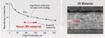
3D Device Technology Development
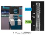
The VLSI Symposium on Technology and Circuits provides a deep dive on recent technical advances, as well as a view into the research efforts that will be transitioning to production in the near future. In a short course presentation at the Symposium, Marko Radosavljevic, from the Components Research group at Intel, provided … Read More
A Crisis in Engineering Education – Where are the Microelectronics Engineers?

At the recent VLSI Symposium on Technology and Circuits, a panel discussion presented a jarring forecast. The theme of the panel was “Building the 2030 Workforce: How to Attract Great Students and What to Teach Them?”, with participants from academia and industry, as well as a packed (and vocal) audience.
On the one hand, the … Read More
TSMC 2022 Technology Symposium Review – Advanced Packaging Development

TSMC recently held their annual Technology Symposium in Santa Clara, CA. The presentations provide a comprehensive overview of their technology status and upcoming roadmap, covering all facets of the process technology and advanced packaging development. This article will summarize the highlights of the advanced packaging… Read More
TSMC 2022 Technology Symposium Review – Process Technology Development

TSMC recently held their annual Technology Symposium in Santa Clara, CA. The presentations provided a comprehensive overview of their status and upcoming roadmap, covering all facets of process technology and advanced packaging development. This article will summarize the highlights of the process technology updates… Read More
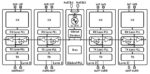
Standardization of Chiplet Models for Heterogeneous Integration
The emergence of 2.5D packaging technology for heterogeneous die integration offers significant benefits to system architects. Functional units may be implemented using discrete die – aka “chiplets” – which may be fabricated in different process nodes. The power, performance, and cost for each unit may be optimized separately.… Read More
Advanced Packaging Analysis at DesignCon
The slogan for the DesignCon conference has been “where the chip meets the board”. Traditionally, the conference has provided a breadth of technical presentations covering the design and analysis of high-speed communication interfaces and power integrity evaluations between chip, board, and system.
The recent DesignCon… Read More
An Update on In-Line Wafer Inspection Technology

From initial process technology development (TD) to high volume manufacturing (HVM) status for a new node, one of the key support functions to improve and maintain yield is the in-line wafer inspection technology. Actually, there are multiple inspection technologies commonly employed, with tradeoffs in pixel resolution,… Read More
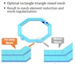
Inverse Lithography Technology – A Status Update from TSMC
“Inverse lithography technology (ILT) represents the most significant EDA advance in the last two decades.” Danping Peng from TSMC made that assertion at the recent SPIE Advanced Lithography + Patterning Conference, in his talk entitled: ILT for HVM: History, Present, and Future. This article summarizes the highlights… Read More


TSMC CoWoS versus Intel EMIB Semiconductor Packaging