TSMC recently held their annual Technology Symposium in Santa Clara, CA. The presentations provide a comprehensive overview of their technology status and upcoming roadmap, covering all facets of the process technology and advanced packaging development. This article will summarize the highlights of the advanced packaging technology presentations – a previous article covered the process technology area.
General
TSMC has merged their 2.5D and 3D packaging offerings into a single brand – “3D Fabric”. The expectations are that there will be future customers that pursue both options to provide dense, heterogeneous integration of system-level functionality – e.g., both “front-end” 3D vertical assembly, combined with “back-end” 2.5D integration.
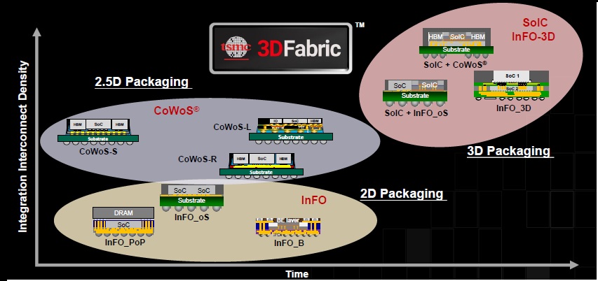
Technically, the 2.5D integration of SoCs with “3D” high-bandwidth memory HBM stacks is already a combined offering. As illustrated above, TSMC is envisioning a much richer mix of topologies in the future, combining 3D SoIC with 2.5D CoWoS/InFO as part of very complex heterogeneous system designs.
As with the process technology presentations at the Symposium, the packaging technology updates were pretty straightforward – an indication of successful, ongoing roadmap execution. There were a couple of specific areas representing new directions that will be highlighted below.
Of particular note is the TSMC investment in an Advanced System Integration fab, which will support the 3D Fabric offerings, providing full assembly and test manufacturing capabilities.
2.5D packaging
There are two classes of 2.5D packaging technologies – “chip-on-wafer-on-substrate” (CoWoS) and “integrated fanout” (InFO).
(Note that in the figure above, some of the InFO offerings are denoted by TSMC as “2D”.)
The key initiative for both these technologies is to continue to expand the maximum package size, to enable a larger number of die (and HBM stacks) to be integrated. As an example, the fabrication of the interconnect layers on a silicon interposer (CoWoS-S) requires “stitching” multiple lithographic exposures – the goal is to increase the interposer size in term of multiples of the maximum reticle dimensions.
- CoWoS
CoWoS has expanded to offer three different interposer technologies (the “wafer” in CoWoS):
- CoWoS-S
- uses a silicon interposer, based on existing silicon wafer lithographic and redistribution layer processing
- in volume production since 2012, >100 products for 20+ customers to date
- the interposer integrates embedded “trench” capacitors
- 3X max reticle size in development – to support a design configuration with 2 large SoC’s and 8 HBM3 memory stacks, with eDTC1100 (1100nF/mm**2)
- CoWoS-R
- uses an organic interposer for reduced cost
- up to 6 redistribution layers of interconnect, 2um/2um L/S
- 2.1X reticle size supporting one SoC with 2 HBM2 stacks in a 55mmX55mm package; 4X reticle size in development, with 2 SoCs and 2HBM2 in an 85mmX85mm package
- CoWoS-L
- uses a small silicon “bridge” inserted into an organic interposer, for high density interconnects between adjacent die edges (0.4um/0.4um L/S pitch)
- 2X reticle size supports 2 SoCs with 6 HBM2 stacks 2023); 4X reticle size in development to support 12 HBM3 stacks (2024)
TSMC highlighted that they are working with the HBM standards group on the physical configuration of HBM3 interconnect requirements for CoWoS implementations. (The HBM3 standard appears to have settled on the following for the stack definition: capacity of 4GB w/four 8Gb die to 64GB w/sixteen 32Gb die; 1024-bit signal interface; up to 819GBps bandwidth.) These upcoming CoWoS configurations with multiple HBM3 stacks would provide tremendous memory capacity and bandwidth.
Also, in anticipation of much greater power dissipation in upcoming CoWoS designs, TSMC is working on appropriate cooling solutions, both improved thermal-interface-materials (TIM) between die and package, as well as transitioning from air to immersion cooling.
- InFO
After accurate (face-down) placement orientation on a temporary carrier, die are encapsulated in a epoxy “wafer”. Redistribution interconnect layers are added to the reconstituted wafer surface. The package bumps are then connected directly to the redistribution layers.
There are InFO_PoP, InFO_oS, and InFO_B topologies.
As shown below, InFO_PoP denotes a package-on-package configuration, and is focused on integration of a DRAM package with a base logic die. The bumps on the DRAM top die utilize through-InFO vias (TIV) to reach the redistribution layers.

- InFO_PoP primarily for the mobile platform
- over 1.2B units shipped since 2016
An issue with the InFO_PoP implementation is that currently the DRAM package is a custom design, and only able to be fabricated at TSMC. There is an alternative InFO_B topology in development, where an existing (LPDDR) DRAM package is added on top, with assembly to be provided by an external contract manufacturer.
InFO_oS (on-substrate) enables multiple die to be encapsulated, with the redistribution layers and their microbumps connected to a substrate with TSVs.
- in production for over 5 years, focus is on HPC customers
- 5 RDL layers on the substrate, with 2um/2um L/S
- the substrate enables a large package footprint, currently at 110mm X 110mm with plans for greater sizes
- 130um C4 bump pitch

As depicted above, InFO_M is an alternative to InFO_oS, with multiple encapsulated die and redistribution layers, without the additional substrate + TSVs (< 500mm**2 package, production in 2H2022).
3D packaging
InFO-3D
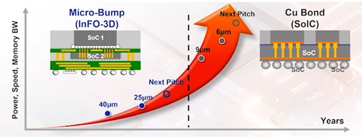
There is a 3D stacked package technology that utilizes micro-bumped die integrated vertically with redistribution layers and TIVs, focused on the mobile platform.
3D SoIC
The more advanced vertical-die stacked 3D topology packaging family is denoted as “system-on-integrated chips” (SoIC). It utilizes direct Cu bonding between the die, at an aggressive pitch.
There are two SoIC offerings – “wafer-on-wafer” (WOW) and “chip-on-wafer” (COW). The WOW topology integrates a complex SoC die on a wafer providing deep trench capacitor (DTC) structures for optimal decoupling. The more general COW topology stacks multiple SoC die.
The process technologies qualified for SoIC assembly are shown in the table below.
 Design Enablement for 3DFabric, including 3Dblox
As illustrated in the upper right corner of the 3D Fabric image above, TSMC is envisioning complex system design-in-package implementations, combining both 3D SoIC and 2.5D technologies.
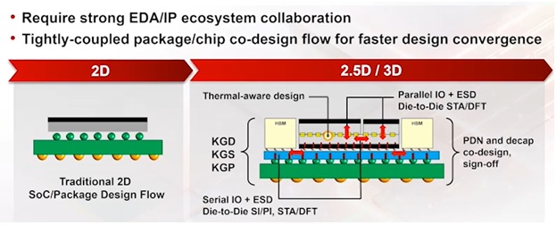
The resulting complexity in the design flow is great, as highlighted above, with advanced thermal, timing, and SI/PI analysis flows required (which can also deal with the model data volume).
To enable the development of these system-level designs, TSMC has collaborated with EDA vendors on three major design flow initiatives:
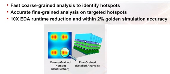
- improved thermal analysis, using a coarse-grained plus fine-grained approach)
- hierarchical static timing analysis
- individual die are represented by an abstracted model, to reduce the total (multi-corner) data analysis complexity
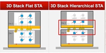
- individual die are represented by an abstracted model, to reduce the total (multi-corner) data analysis complexity
- front-end design partitioning
To help accelerate the front-end design partitioning of a complex system, TSMC has pursued an initiative denoted as “3Dblox”.
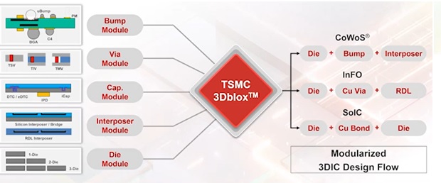
The goal is to break down the overall physical package system into modular components, which are then integrated. The module categories are:
- bumps/bonds
- vias
- caps
- interposers
- die
These modules would be incorporated into any of the SoIC, CoWoS, or InFO package technologies.
Of specific note is that TSMC is driving an effort to enable 3D Fabric designs to use various EDA tools – that is, to complete physical design with one EDA vendor tool, and (potentially) use different EDA vendor products for support for timing analysis, signal integrity/power integrity analysis, thermal analysis.
3Dblox appears to take the concept of “reference flows” for SoCs to a new level, with TSMC driving interoperability between EDA vendor data models and formats. The overall 3Dblox flow capability will be available in 3Q2022. (A preliminary step – i.e., automated routing of redistribution signals on InFO – will be the first feature released.)
Clearly, TSMC is investing extensively in advanced packaging technology development and (especially) new fabrication facilities, due to the anticipated growth in both 2.5D and 3D configurations. The transition from HBM2/2e to HBM3 memory stacks will result in considerable performance benefits to system designs utilizing CoWoS 2.5 technology. Mobile platform customers will expand the diversity of InFO multi-die designs. The adoption of complex 3DFabric designs combining both 3D and 2.5D technologies will no doubt increase, as well, leveraging TSMC’s efforts to “modularize” the design elements to accelerate system partitioning, as well as their efforts to enable a broad set of EDA tools/flows to be applied.
-chipguy
Also Read:
TSMC 2022 Technology Symposium Review – Process Technology Development
Three Key Takeaways from the 2022 TSMC Technical Symposium!
Inverse Lithography Technology – A Status Update from TSMC
Share this post via:


Comments
2 Replies to “TSMC 2022 Technology Symposium Review – Advanced Packaging Development”
You must register or log in to view/post comments.