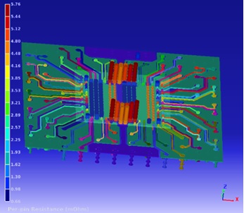
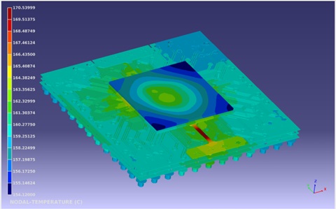
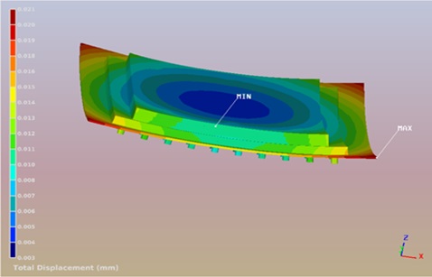
Semiconductor manufacturers are under constantly increasing and intense pressure to accelerate innovative new chip designs to market faster than ever in smaller package sizes while assuring signal integrity and reducing power consumption. Three-dimensional integrated circuits (3D-ICs) promise to answer all these demands but, at the same time, they introduce a new level of design complexity that is challenging traditional tools and processes.
Manufactured by stacking dies and interconnecting them so they perform as a single device, 3D- ICs create new risks, including thermal build-up caused by greater density. Because they’re significantly larger than a typical system-on-a-chip (SoC), with longer interconnects, they need to be rigorously tested for faulty integration points as well as system-level failures.
However, most semiconductor development teams simply aren’t equipped to manage the difficult job of 3D-IC analysis and design validation. They’re burdened by a historical approach to SoC simulation that relies on a serial, step-by-step process, in which single-physics simulation tools are applied one by one. When engineers apply these disparate tools, and this serial process, to complex 3D-IC designs, they’re missing system-level interactions, connection points, consolidated thermal effects and other considerations for something to go seriously wrong.
As 3D-ICs become more common for advanced semiconductor applications, engineering teams need a new analytic approach that’s equally innovative. They need a single, open and proven platform to conduct concurrent, multivariate simulation and analysis across the entire product design. They need to consider multiple physics, quickly and simultaneously, at both the component and system levels.
An Open Platform for Optimizing Every Performance Aspect
Ansys’ industry-leading solutions for 3D-IC simulation and analysis provide engineering teams with best-in-class capabilities for optimizing every aspect of performance, including power integrity, reliability, electromagnetics (EM), thermal, computational fluid dynamics (CFD) and mechanical stress.

The comprehensive Ansys toolkit positions semiconductor engineering teams to assess stand-alone performance aspects like thermal conductivity, while simultaneously looking at every other critical metric. The entire 3D-IC design can be subjected to realistic operating conditions as an integrated system, beginning at the earliest design stage.

Ansys provides a unified 3D-IC simulation platform incorporating our best-in-class solutions. For example, Ansys RedHawk-SC Electrothermal can be leveraged to verify the thermal hotspots, melting risk, local failure modes of each welding site, based on the electrical current load at that specific point. Ansys CFD capabilities can optimize the performance of fans and heat sinks as they generate airflows to cool the assembly. Ansys solutions can also analyze advanced performance aspects, such as low-frequency power oscillations, and predict their impact on the larger design.

Not only does Ansys address all of these individual engineering challenges through best-in-class solvers, but it equips semiconductor development teams to conduct these studies simultaneously. Only Ansys supports this type of multiphysics, multivariate, concurrent approach that reveals critical design trade-offs at the system level, rapidly and at an early stage.
In Your Rush to Market, Don’t Shortchange Your Analysis
Faced with worldwide chip shortages, increasing performance demands, a lack of engineering talent, and an urgent need for low-cost innovation, semiconductor manufacturers may be tempted to focus on their existing set of serial processes and isolated, single-physics simulation tools. But these outdated methods are insufficient to capture the complexity of 3D-IC designs and their equally complex failure risks.
Different engineers, using different simulation and analysis tools, may actually work at cross-purposes. For instance, one team’s efforts to resolve a signal-integrity issue might inadvertently create a timing failure or thermal risk that needs to be resolved by another team — which then hands it back to the signal-integrity team. The result? The dreaded ping pong effect with costly delays, resource-intensive handoffs, and significant rework.
In contrast, the robust and comprehensive Ansys simulation platform supports synergistic, collaborative, and cross functional analysis. It’s fast and intuitive for the multidisciplinary design team to look at the holistic 3D-IC design and concurrently analyze novel physics, to optimize performance aspects from electrical reliability to mechanical and thermal stability.
Collaboration-Driven Innovation: The Wave of the Future
The world’s semiconductor leaders are realizing that true 3D-IC innovation requires a new level of collaboration and vertical integration. Only by removing traditional functional boundaries — and eliminating a single-physics, serial approach — can development teams accelerate the design cycle, drive down costs, and produce game-changing new performance innovations.
Ansys’ open, extensible, and powerful simulation platform for multiphysics 3D-IC simulation is purpose-built to realize this vision. By leveraging a unified platform with proven, best-in-class solutions for multiphysics and multiscale analysis, semi development teams can launch new designs quickly and collaboratively, without sacrificing analytic rigor or product confidence. Costly handoffs and rework are reduced as the cross functional team shares the same understanding of performance trade-offs and ultimate goals.
While it can be difficult to break down cultural and organizational barriers to collaboration and vertical integration, the rewards are well worth it, including faster time-to-market and higher levels of innovation. Replacing sequential analysis and a disparate toolkit with the Ansys platform to support concurrent, multiphysics, system-level design simulations is a critical first step.
Visit Ansys at DAC 2022
If you’re hoping to fully capitalize on the incredible promise of 3D-IC designs, you owe it to yourself to learn more about the Ansys platform for multivariate, multiphysics simulation. Visit Ansys at Booth #1539 at the Design Automation Conference (DAC), in San Francisco July 11-14. Request a meeting or product demo now to start supporting a new level of 3D-IC design optimization.
Also read:
A Different Perspective: Ansys’ View on the Central Issues Driving EDA Today
Unlock first-time-right complex photonic integrated circuits
Take a Leap of Certainty at DAC 2022
Share this post via:


Comments
There are no comments yet.
You must register or log in to view/post comments.