You are currently viewing SemiWiki as a guest which gives you limited access to the site. To view blog comments and experience other SemiWiki features you must be a registered member. Registration is fast, simple, and absolutely free so please,
join our community today!
One of the standout presentations at the 2026 TSMC OIP Forum highlighted a collaboration between Siemens EDA, Marvell, and TSMC. I always appreciate EDA presentations that bring together customer and foundry perspectives, and this one did not disappoint. We follow 3D IC technology closely and have published more than 150 blogs… Read More
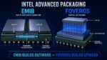
Intel EMIB and Intel Foveros are advanced semiconductor-packaging technologies designed to combine multiple silicon dies, or chiplets, within one processor package. Both support heterogeneous integration: manufacturers can build different functions using the process technology best suited to each one, then connect … Read More
Accellera Systems Initiative invites the design and verification community to join us at the 2026 Design Automation Conference for a focused technical luncheon, “Embracing AI for Advanced Design and Verification,” on Tuesday, July 28, from 12:30–1:45 p.m. at the Long Beach Convention Center, Meeting Room 104C.
Artificial… Read More
Consider this a standout presentation at the Silicon Catalyst Spring Portfolio Update Meeting held yesterday at the Computer History Museum. Mahesh Tirupattur, CEO of Analog Bits, is a modern-day, multidimensional semiconductor hero and one of my trusted few. Analog Bits is a premier member of the semiconductor ecosystem,… Read More
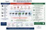
The semiconductor industry has achieved extraordinary mastery in silicon signoff. Modern EDA environments can now optimize timing closure, physical verification, IR/EM behavior, routing density, thermal interaction, and increasingly even design-space exploration through AI-assisted implementation flows. Crossing… Read More
imec announced that IC-Link by imec has joined the TSMC 3DFabric Alliance, a strategically important move that reflects the semiconductor industry’s transition from traditional monolithic scaling toward heterogeneous integration, chiplet architectures, and advanced packaging-driven system optimization. The partnership… Read More
Given the success of the event in Silicon Valley last week, I would expect the Siemens U2U event in Munich to be even bigger. In my experience this has been the best user driven event in 2026 with the deepest customer content. EDA has always been a customer driven industry and it is good to see us recognize that from time to time. Kalar … Read More
TSMC continues to reinforce its leadership in advanced semiconductor manufacturing through its deepening collaboration with Cadence Design Systems. The expanded partnership focuses on enabling next-generation artificial intelligence and high-performance computing innovations by aligning advanced electronic design… Read More
AI, hyperscale data centers, and data-intensive workloads are driving unprecedented demands for performance, bandwidth, and energy efficiency. As the economic returns of traditional transistor scaling diminish, advanced IC packaging and heterogeneous integration have become the primary levers for system-level scaling.… Read More
Socionext’s recent run of rapid 3D-IC tape-outs is a noteworthy milestone for the industry with two successful tape-outs in just seven months for complex, multi-die designs aimed at AI and HPC workloads. That pace of iteration highlights how advanced packaging, richer EDA toolchains, and closer foundry-ecosystem collaboration… Read More