You are currently viewing SemiWiki as a guest which gives you limited access to the site. To view blog comments and experience other SemiWiki features you must be a registered member. Registration is fast, simple, and absolutely free so please,
join our community today!
The worldwide TSMC 2025 Technology Symposium recently kicked off with the first event in Santa Clara, California. These events typically focus on TSMC’s process technology and vast ecosystem. These items were certainly a focus for this year’s event as well. But there is now an additional item that shares the spotlight – packaging… Read More
The main program for the 70th IEDM opened on Monday morning in San Francisco with an excellent keynote from Dr. Yuh-Jier Mii, Executive Vice President and Co-Chief Operating Officer at TSMC. Dr. Mii joined TSMC in 1994. Since then, he has contributed to the development and manufacturing of advanced CMOS technologies in both fab
…
Read More
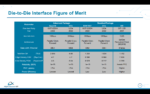
At the 2024 TSMC OIP Ecosystem Forum, one of the technical talks by TSMC focused on maximizing 3DIC design productivity and rightfully so. With rapid advancements in semiconductor technology, 3DICs have become the next frontier in improving chip performance, energy efficiency, and density. TSMC’s focus on streamlining the… Read More
The TSMC Technology Symposium provides a worldwide stage for TSMC to showcase its advanced technology impact and the extensive ecosystem that is part of the company’s vast reach. These events occur around the world and the schedule is winding down. TSMC covers many topics at its Technology Symposium, including industry-leading… Read More
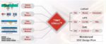
TSMC recently held their annual Technology Symposium in Santa Clara, CA. The presentations provide a comprehensive overview of their technology status and upcoming roadmap, covering all facets of the process technology and advanced packaging development. This article will summarize the highlights of the advanced packaging… Read More
The topic of chiplets is getting a lot of attention these days. The chiplet movement has picked up more momentum since Moore’s law started slowing down as process technology approached 5nm. With the development cost of a monolithic SoC crossing the $500M and wafer yields of large die-based chips dropping steeply, the decision … Read More
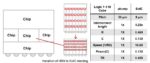
Advanced 2.5D/3D Packaging Roadmapby Tom Dillinger on 01-03-2022 at 6:00 amCategories: Events, Semiconductor, TSMC
Frequent SemiWiki readers are no doubt familiar with the advances in packaging technology introduced over the past decade. At the recent International Electron Devices Meeting (IEDM) in San Francisco, TSMC gave an insightful presentation sharing their vision for packaging roadmap goals and challenges, to address the growing… Read More
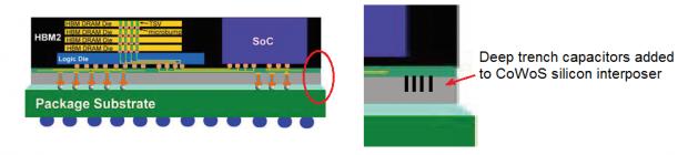
The recent TSMC Technology Symposium provided several announcements relative to their advanced packaging offerings.
General
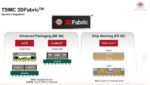
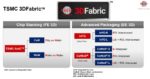
3DFabricTM
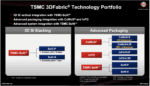
Last year, TSMC merged their 2.5D and 3D package offerings into a single, encompassing brand – 3DFabric.
2.5D package technology – CoWoS
The 2.5D packaging options are divided into the CoWoS… Read More
Recently, TSMC held their 26th annual Technology Symposium, which was conducted virtually for the first time. This article is the second of three that attempts to summarize the highlights of the presentations. This article focuses on the TSMC advanced packaging technology roadmap, as described by Doug Yu, VP, R&D.
Key… Read More
TSMC recently held their annual Technology Symposium in Santa Clara. Part 1 of this article focused on the semiconductor process highlights. This part reviews the advanced packaging technologies presented at the symposium.
TSMC has clearly made a transition from a “pure” wafer-level foundry to a supplier of complex integrated… Read More