You are currently viewing SemiWiki as a guest which gives you limited access to the site. To view blog comments and experience other SemiWiki features you must be a registered member. Registration is fast, simple, and absolutely free so please,
join our community today!
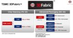
Recently, TSMC held their 26th annual Technology Symposium, which was conducted virtually for the first time. This article is the second of three that attempts to summarize the highlights of the presentations. This article focuses on the TSMC advanced packaging technology roadmap, as described by Doug Yu, VP, R&D.
Key… Read More
TSMC recently held their annual Technology Symposium in Santa Clara. Part 1 of this article focused on the semiconductor process highlights. This part reviews the advanced packaging technologies presented at the symposium.
TSMC has clearly made a transition from a “pure” wafer-level foundry to a supplier of complex integrated… Read More
In constant pursuit of improved performance, power and cost, chip and system designers always want to integrate more functions together because this minimizes inter-device loads (affecting performance and power) and bill of materials on the board (affecting cost). However it generally isn’t possible to integrate … Read More
At the TSMC Technology Symposium last month Suk Lee presented a lot of information on design enablement. Suk is an interesting guy with a unique background in ASIC, Semiconductor, EDA, and now Foundry. In baseball terms that would be like playing infield, outfield, home plate, and umpire!
Around the turn of the millennium Suk actually… Read More
Today was TSMC’s 2015 North American Technology Symposium. They talked about a lot of things but perhaps the most important was that they gave a lot of details of new processes, new fabs, and volume ramps.… Read More