“Inverse lithography technology (ILT) represents the most significant EDA advance in the last two decades.” Danping Peng from TSMC made that assertion at the recent SPIE Advanced Lithography + Patterning Conference, in his talk entitled: ILT for HVM: History, Present, and Future. This article summarizes the highlights of his insightful presentation. Indeed, ILT has enabled improvements in the ability to print wafer-level features with improved fidelity.
ILT History
First, a brief review of the steps after design tapeout, associated with mask manufacture:
- The mask shop applies optical proximity correction (OPC) or ILT algorithms to the mask data.
- Mask data prep (MDP) will compose the OPC/ILT-generated data in a format suitable for the mask writer.
- Mask writing has evolved from (an optically-based) pattern-generation shot exposure of the photoresist-coated mask blank to an e-beam based exposure. Both variable-shaped beam (VSB) and multiple-beam ask writing systems are available. (More on this shortly.)
- Mask inspection steps include:
- critical dimension (CD) metrology (CD-SEM)
- mask review using an aerial image measurement system (e.g., Zeiss AIMS)
- mask defect repair
The mask then proceeds to the fab, where a wafer-level print will be subjected to similar steps: CD-SEM dimensional evaluation, wafer inspection and defect analysis.
The need for mask correction algorithms is highlighted in the figure below.
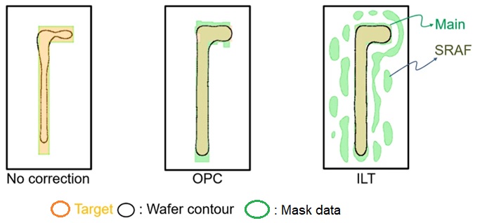
As the printed dimensions on the wafer scaled with successive process nodes, the fidelity of the image – i.e., the difference between the target image and the printed wafer contour – became poor. Corrections to the layout design data were needed.
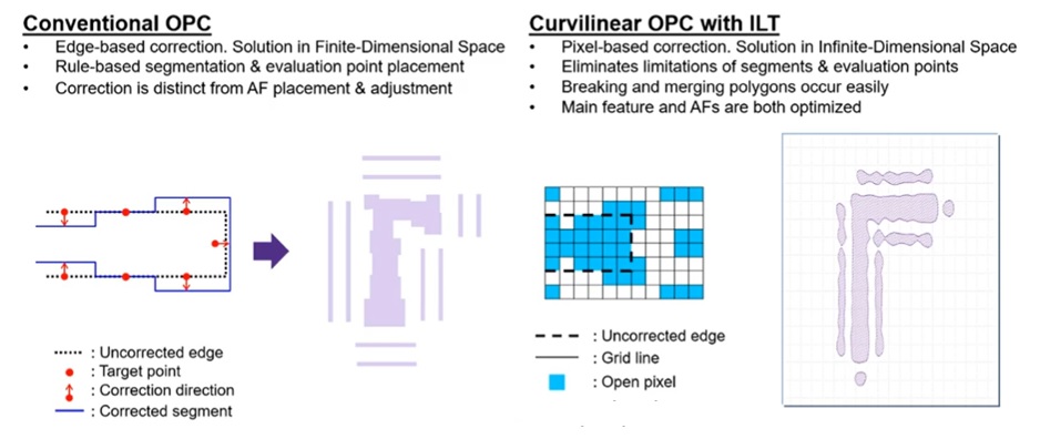
The original approach to generating mask updates were denoted as optical proximity corrections (OPC). Individual segments in the (rectilinear) design data were bisected at appropriate intervals, and the sub-segments were moved, typically using a rule-based algorithm. Rectangular serifs were added at shape corners – both expanded segments at outside corners and reduced at inside corners. (Colorful names were given to the OPC results – e.g., “hammerheads”, “dogbones”.)
Subsequently, OPC algorithms added sub-resolution assist features (SRAF) to the mask data. These are distinct shapes from the original design, whose dimension is intentionally chosen so as not to print at the wafer photoresist resolution, but to provide the appropriate (constructive and destructive) interference due to optical diffraction at the edges of the design shapes.
As shown in the figures above and below, ILT algorithms make a fundamentally different assumption, utilizing curvilinear mask data for corrections and SRAFs. The figure below illustrates the key differences between the edge-based nature of OPC and the pixel-based ILT algorithm.
How ILT Works
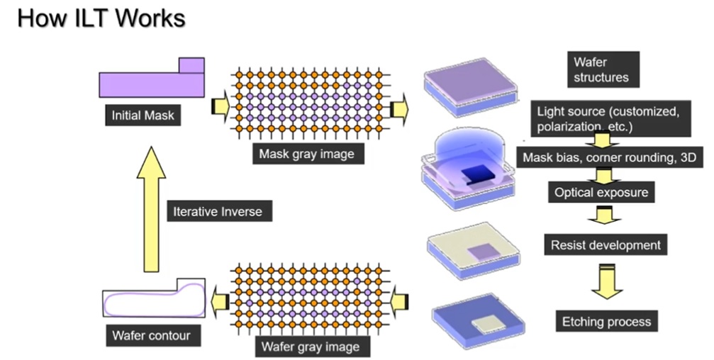
Danping used the following two figures to illustrate how ILT works. The first figure below is a high-level flowchart, providing the comprehensive (ideal) iterative loop between mask data generation and post-etch wafer-level metrology. (More on this full loop shortly.)
The figure below provides more detail on the ILT flow. Two adjacent shapes are used for illustration.
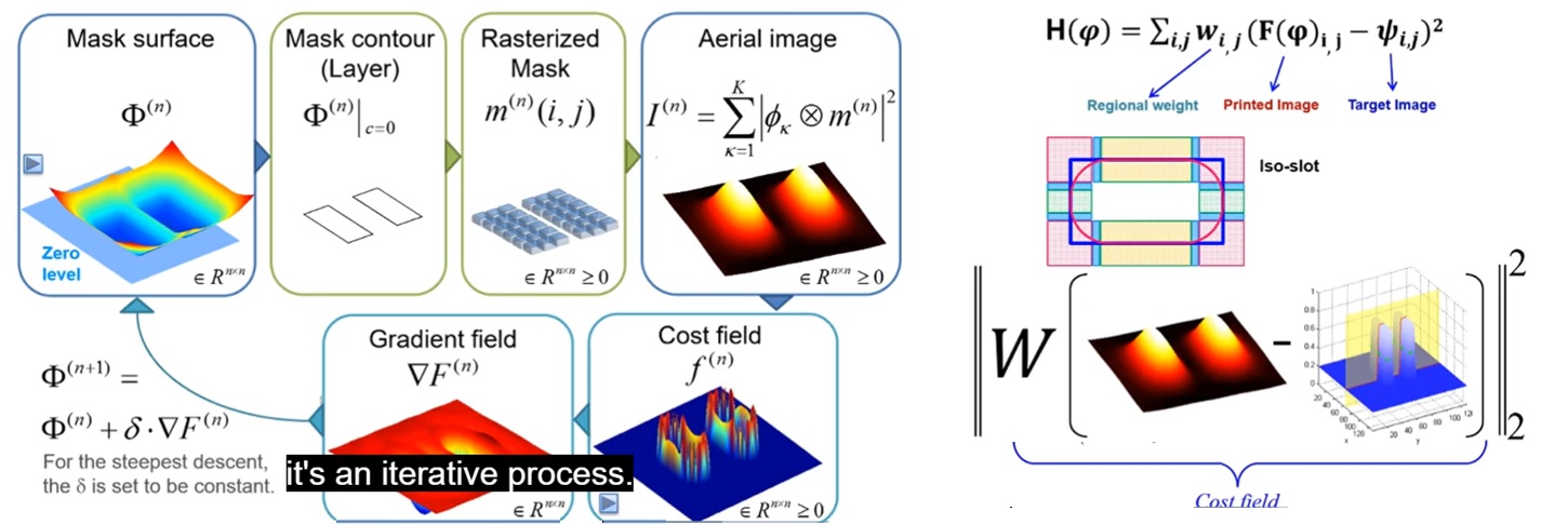
A three-dimensional representation of the illumination intensity is computed. An error function is calculated, with a weighted sum of constituent elements. Each weight is multiplied by a factor related to the difference between the calculated print image and the wafer target across the pixel field.
The error function could include contributions from a variety of printed image characteristics:
- nominal dimension (print-to-target difference)
- modeled three-dimensional resist profile
- pixel light intensity outside the target area to be suppressed
- sensitivity to illumination dose and focus variations
Iterative optimizations are pursued to reduce the magnitude of this error function. Note that the figure above mentions gradient-based optimization to reduce the error function calculated form a difference between a model prediction and a target – the similarities of ILT to machine learning methods are great, as Danping highlighted in the Futures portion of his talk.
Current ILT Adoption and Challenges
There have been hurdles to ILT adoption over the past two decades. Danping reviewed these challenges, and how they are being addressed.
- mask write time
The curvilinear (pixel-based) ILT mask data provide improved depth-of-focus over conventional OPC methods. Yet, the corresponding data complexity results in a major increase in the e-beam shot count to write the mask, using variable size beam (VSB) technology.
Danping explained, “When ILT was first being pursued, there were no multiple beam mask writers. As a result, it took days to expose an ILT mask with a VSB system. Now, with multiple-beam systems, the mask write time in essentially constant, around 8 hours.”
Note that there are “moderate constraints” applied for the ILT data generation to assist with this speed-up – e.g., minimum design rules for SRAF area/space/CD, maximum limits on the curvature of the shapes data.
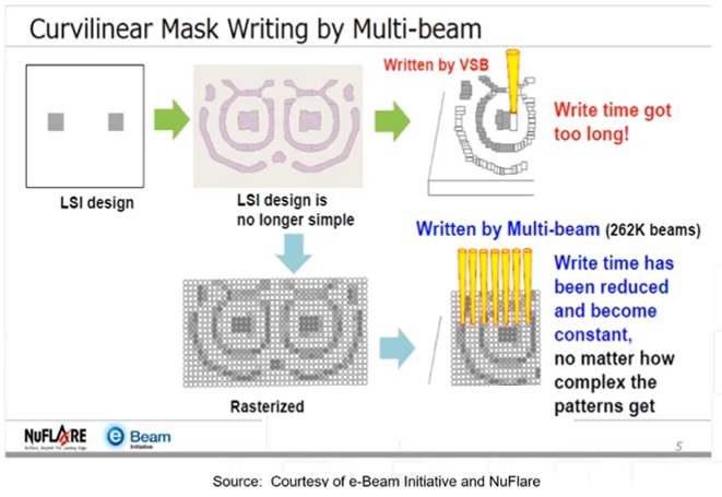
- ILT mask data generation time
“The first adoption of ILT was by memory foundries.”, Danping indicated. “The highly repetitive nature of their layouts, with some careful crafting, results in a reduced number of repeating patterns.”
ILT adoption for logic designs has been slower. Danping elaborated on some of the challenges:
-
- long computational runtime (“20X slower than OPC”)
- mask data rules checking technology for curvilinear edges has lagged
- improvements in exposure systems have improved image resolution (e.g., 193 to 193i) and dose uniformity, reducing the ILT advantages
ILT algorithms for model generation and error function + gradient computation is dominated by matrix operations. To address the runtime challenge, ILT code has been ported to GPU-based computation resources. This provides “a 10X speed-up over strictly CPU-based computation”, according to Danping.
To address the mask data validation challenge, the SEMI Curvilinear Task Force is working on a data representation that will serve as a standard format for model interchange. (This is also driven by the curvilinear design layout data associated with silicon photonics structures.) The figure below illustrates new “rule definitions” that will be part of mask data checking.
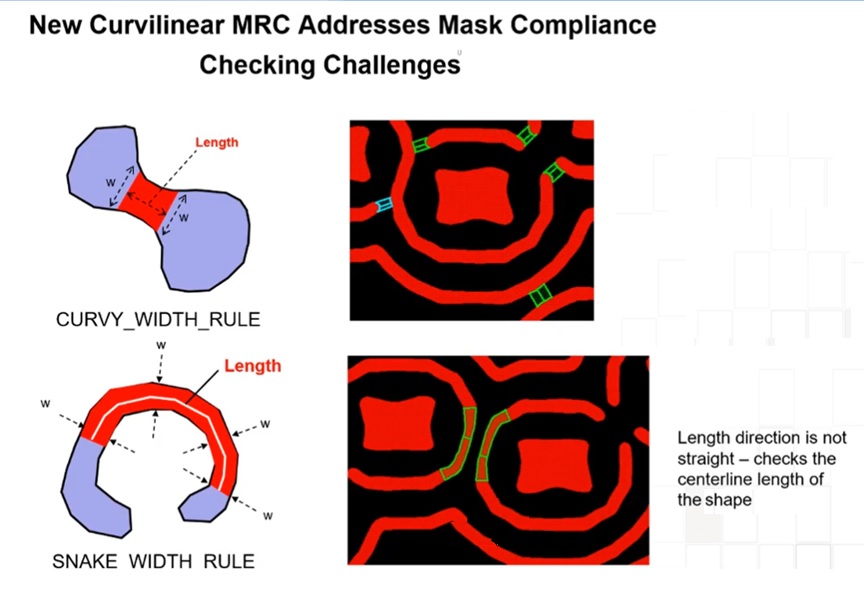
Danping provided the following observation on the market opportunity for ILT relative to improvements in exposure systems, “ILT can be used to squeeze more performance from an existing tool.” In that sense, ILT may enable extended utilization of existing scanners.
Danping shared a forecast that “Both EUV and 193i masks will commonly incorporate curvilinear shapes in 2023.” (Source: eBeam Initiative)
ILT Future
Danping offered three forecasts for ILT technology.
- adoption of deep learning techniques
As mentioned above, the ILT algorithm shares a great deal in common with the computation and optimization techniques of deep neural network methods. The figure below illustrates how deep learning could be adopted.
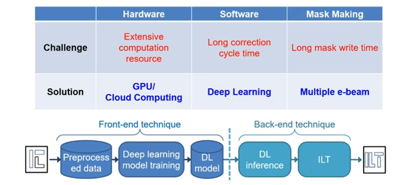
“A trained deep learning model could be used to generate mask data, followed by a small number of ILT iterations. ILT mask data could be derived in 15% of the previous runtime.”, Danping mentioned.
- increased use of curvilinear design data
In addition to silicon photonics structures, the opportunity to use curvilinear data directly in circuit layouts at advanced process nodes may soon be adopted. (Consider the case where metal “jumpers” are used on layer Mn+1 to change routing tracks for a long signal on layer Mn.) The industry support for curvilinear data representation would enable this possibility, although it would also have a major impact on the entire EDA tool flow.
- a full “inverse etch technology” (IET) flow to guide ILT
An earlier figure showed a “full loop” flow for mask data generation, incorporating post-etch results. Rather than basing the ILT error function on computational models of the resist expose/develop profile, the generation of the cost function would be derived from the final etched material image model, as illustrated below.

(DOM: dimension of mask; ADI: after photoresist develop inspection; AEI: after etch inspection)
Significant effort would be needed to construct the “digital twin” models for etch processes. However, the benefits of a comprehensive mask data-to-process flow optimization would be great.
Summary
ILT will clearly expand beyond its current (memory-focused) applications. The industry efforts to support a standard for efficient and comprehensive curvilinear data representations – for both mask and design data – will help to accelerate the corresponding EDA and fabrication equipment enablement. As Danping put it, “It is not a question of if, but when and how many layers will use ILT.”
-chipguy
Also Read:
TSMC N3 will be a Record Setting Node!
Share this post via:


Comments
6 Replies to “Inverse Lithography Technology – A Status Update from TSMC”
You must register or log in to view/post comments.