
The quest for bigger FPGA-based prototyping platforms continues, in lockstep with each new generation of faster, higher capacity FPGAs. The arrival of the Xilinx Virtex UltraScale+ VU19P FPGA takes capacity to new levels and adds transceiver and I/O bandwidth. When these slot into S2C’s Prodigy S7-19P Logic System, the result is flexible ASIC and SoC prototyping for validation and firmware workflows. Let’s look at FPGA-based prototyping for these use cases.
Automated partitioning and realistic high-speed I/O for validation
Hardware teams get concerned when designs must be modified to be tested. Modifications take time and introduce the possibility for errors. FPGA-based prototyping is now mature technology. Firms like S2C have put in years of research on accurately partitioning logic into interconnected FPGAs with automated tools. Improvements in FPGA transceiver bandwidth – up to 4.5Tb/s total in the VU19P – streamline SerDes interconnects between parts for minimal latency.
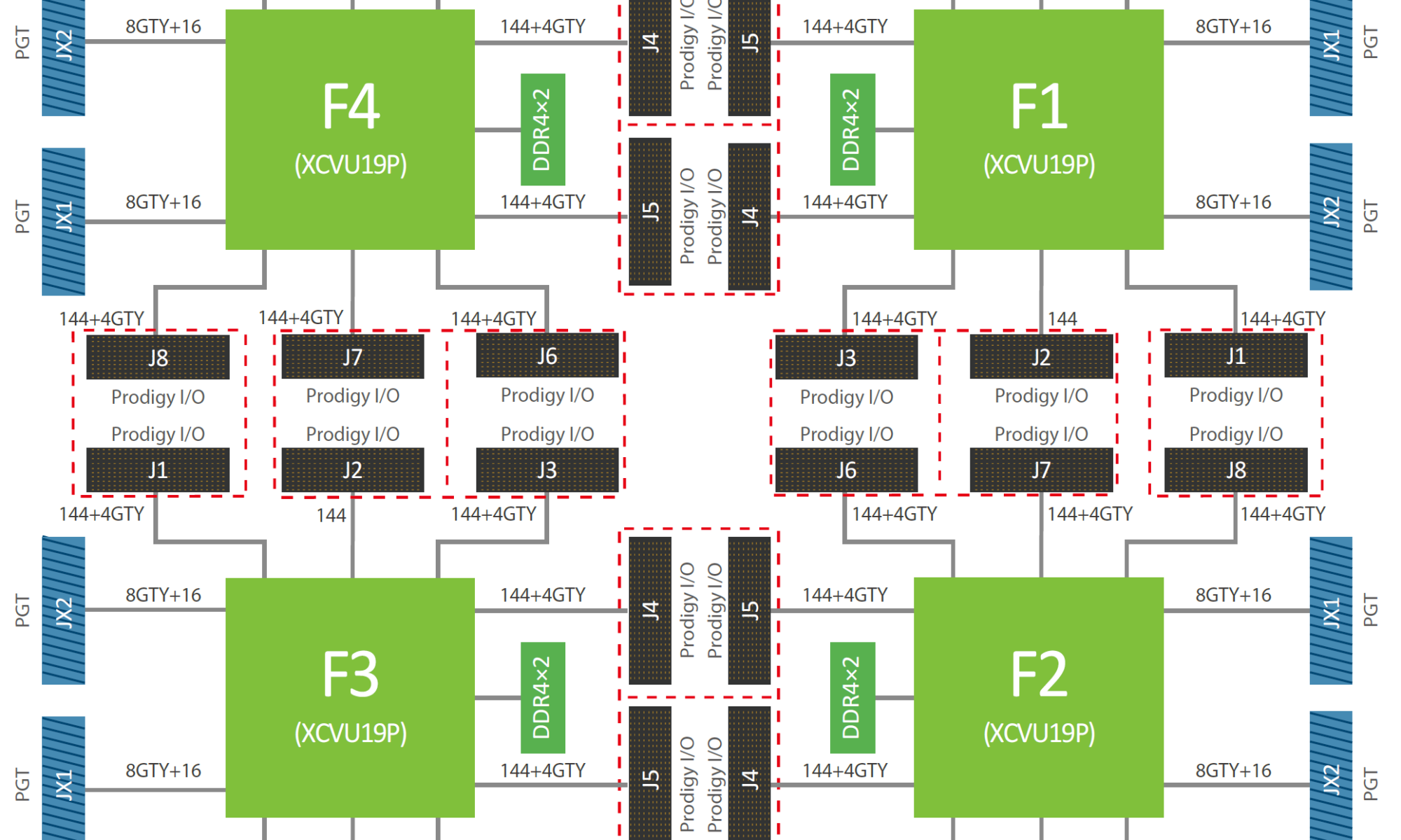
With four VU19Ps, the 7th-generation Prodigy S7-19PQ can take on ASIC and SoC designs of up to 196M gates. Teams can scale down with smaller configurations using one or two VU19P FPGAs or scale up by stacking systems and interconnecting logic modules. All interconnects between FPGAs use the same high-speed transceivers, so stacking is as simple as cabling. On-board DDR4 memory keeps the FPGAs fed at speed. Advanced clock management keeps both standalone and multi-system configurations in sync.
During system validation, realistic high-speed I/O for stimulus and output evaluation is a requirement. Often, the burden on teams to create their own I/O testing hardware, S2C has standardized its I/O and created over 90 daughtercards with pre-tested, proven designs. I/O voltages are adjustable in software with steps from 1.2V to 1.8V. Using the same interface, teams can turn to S2C or design their own if a full-custom I/O card is required.

Instead of leaving validation to the very end of the project, and perhaps getting surprised, teams can move to a more continuous validation workflow using FPGA-based prototyping. This also allows room for expanding validation testing, since it’s not compressed into a small window. System-level faults can be exposed earlier and corrected in the ASIC or SoC design.
More power and control in the hands of firmware developers
One of the more powerful use cases for FPGA-based prototyping technology is firmware development for SoCs. For enhanced productivity, software teams need a dedicated system an individual developer can configure and control.
With daughter cards and cables plugged in, the Prodigy S7-19P auto detects its configuration. Designs load into the FPGAs through Ethernet, USB, JTAG, or a microSD card. Developers can kick the box when they need to remotely, powering it on or off or resetting it over Ethernet. A virtual UART allows a developer into firmware for debugging. Virtual switches and LEDs make it easy to change settings and see status remotely.
This kind of power can put software teams on their own workflow track, out of the way of ASIC or SoC hardware teams. Conflicts early in the design, when hardware is in flux and access is tight, can set software schedules behind. Without the right firmware for initializing registers across the chip, hardware progress may slow as well. Firmware developers can start code on a working configuration, reset the platform when they need to, and even reconfigure the platform from a design file stored on the network without bothering the hardware teams.
Win by speeding up surrounding validation and firmware workflows
Most semiconductor IP is thoroughly rung out before it gets into the hands of ASIC and SoC developers. And the tools for combining IP into a design and debugging it are much better. The remaining long poles in the tent are now validation and firmware workflows – and speeding those up with FPGA-based prototyping technology can be a huge win. Platforms like the S2C Prodigy S7-19 Logic System give validation and firmware teams their own environment working in parallel with hardware development. A short S2C video highlights this new platform.
Also read:
White Paper: Advanced SoC Debug with Multi-FPGA Prototyping
Prototype enables new synergy – how Artosyn helps their customers succeed
S2C’s FPGA Prototyping Solutions
Share this post via:


Comments
There are no comments yet.
You must register or log in to view/post comments.