
There is no shortage of reporting on the many technological advances happening within the semiconductor industry. But sometimes it feels like we hear less in the area of semiconductor manufacturing equipment than in the design and product arenas. That doesn’t mean that there is less happening there or what is happening there is of any less value. In fact, the advances or hurdles thereof determine the course of the entire semiconductor industry.
The never ending push for packing more transistors into a sq.mm area of a wafer continues to drive the need for reducing feature sizes. Advanced manufacturing technology is what makes these finer and finer feature sizes possible. Naturally, advanced manufacturing equipment are needed to produce these advanced chips. With many more end-markets creating demands for advanced process-based chips than ever before, wafer fab equipment sales are growing rapidly. According to SEMI, worldwide sales of semiconductor manufacturing equipment in 2021 rose 44% to an all-time record of $102.6 billion.
While fab equipment vendors see huge market opportunities, they also have to address many challenges to deliver cost-effective equipment optimized for mass production use. I recently conversed with Richard Cousin, an Industry Process Expert in Electromagnetics within the SIMULIA Brand line of Dassault Systèmes, headquartered in France. Richard is currently leading the Charged Particle Dynamics driven products and has a strong expertise on vacuum electron devices and plasma physics. The conversation focused on the etching process, which is one of the many steps involved in the manufacture of semiconductor chips. Richard discussed the challenges with the etching process, the designing of advanced plasma reactors and the plasma reactor device workflow. And he closed the conversation with a teaser of how simulation tools at the Fabrication process level can help address the plasma reactor design challenges. This article is a summary of that conversation. For those interested in learning more specifics about the simulation tools, you may want to register for a June 8th Webinar. In that webinar, Richard will dive into the details of simulation and optimization techniques that designers of semiconductor manufacturing equipment will find useful.
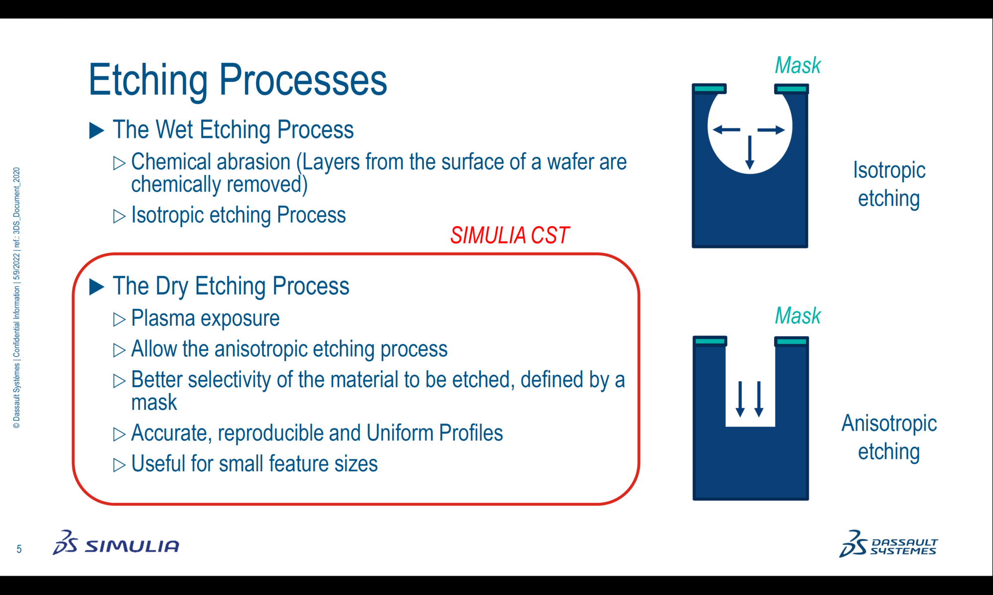
Etching Process: Wet vs Dry
The wet etching process is commonly used for isotropic etching whereas the dry etching process allows anisotropic etching as well as isotropic etching. While the wet etching process is still in use, the chemical reactions can cause issues when radicals are expanded over the device.

With the dry etching process using the Argon neutral gas, there are no chemical reactions. The process is controlled by the plasma uniformity and offers a better selectivity of the material to be etched. The resulting anisotropic etching process is well suited for small size features in the nanoscale. Also, more physical parameters can be controlled to characterize the plasma, such as the input power as well as the pressure of the neutral gas which controls the plasma density. Tuning the operating frequency is set by a so-called matching box.
Thus, the dry etching technique offers better flexibility for delivering accurate and uniform profiles well suited and more critical for small size features.
Designing a Plasma Reactor for Dry Etching
The design of a plasma reactor has to balance many different parameters to accommodate various requirements and plasma characteristics. The plasma characteristics include the density profiles, the ionization rate, the effect of the pressure and the type of gas used as well as the influence of the geometry to prevent damages. One key parameter is the matching network connected to the plasma reactors in order to maximize the input power to be transmitted to the device. This is a critical requirement to maintain the discharge and for better control of the plasma formation for the type of etching to be performed.
Referring to the Figure below, there are different types of dry etching processes that broadly fall into the IBE and RIE categories. The IBE process is a deposition process similar to a sputtering approach whereas the RIE process removes some materials from the substrate. Therefore, the pressures involved in RIEs are more important and require higher plasma densities to etch the substrates. Thus, the designing of a plasma reactor is challenging as it needs to support different types of dry etching processes.

3DS SIMULIA Space Charge Dynamics Simulation Tool
SIMULIA possesses an unique capability of calculating the space charge dynamics for predicting experimental results when no diagnostics are available. The SIMULIA approach allows for virtual prototyping which helps with designing real and new plasma reactors from the space charge dynamics computation to the appropriate RF matching network.
When simulating, SIMULIA can do a microscopic approach or a macroscopic approach. Under the microscopic approach, it uses a time-domain kinetic approach with a Poisson based Particle-In-Cell code. Several particle interactions are taken into account in a global Monte-Carlo Collision (MCC) type model. The ionization of the neutral gas, its excitation and the elastic collisions are considered simultaneously to compute the plasma kinetics. Under its macroscopic approach, SIMULIA treats the plasma as bulk. The plasma parameters are extracted from the MCC models to feed an equivalent dispersion model. This enables it to accurately characterize the matching network (so-called matching box) connected to the plasma reactor.
The SIMULIA space charge dynamics simulation tool simulates all phases of the plasma reactor device workflow except phase 7 (Refer to Figure below).

For those interested in learning more specifics about the simulation tools, you may want to register for a June 8th Webinar.
Also Read:
Executable Specifications Shorten Embedded System Development
Fully Modeling the Semiconductor Manufacturing Process
Optimizing High Performance Packages calls for Multidisciplinary 3D Modeling
Share this post via:


Consolidation and Competition: Who is Winning the $4.5 Billion Interface IP Race?