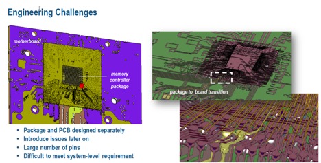

For all the time we spend thinking and talking about silicon design, it’s easy to forget just how important package design is. Semiconductor packages have evolved over the years from very basic containers for ICs into very specialized and highly engineered elements of finished electronic systems. They play an important role in every aspect of chip operation. New packaging technologies, such as 3D IC, SiP, etc., have actually made packages integrated to chip operation. Package design and analysis is becoming more critical because packages can strongly influence cost, reliability, performance, area and a host of other characteristics.
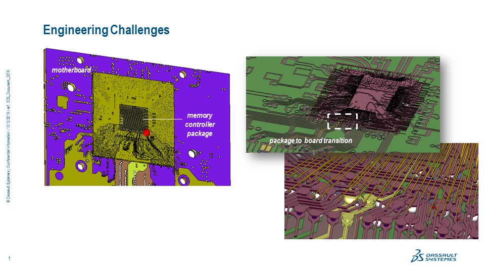
The list of “care abouts” for package design has become pretty long and without a doubt calls for a multidisciplinary approach. Packages essentially are the cocoon that protects the IC die from the effects of its environment. Outside the package there can be threats from moisture and physical shock and vibration. The package also plays a critical role in removing thermal energy away from the IC. Due to expansion and contraction of materials with different CTEs, thermal stress arises at material interfaces in the package. Ultimately, this stress can cause fractures and cracking, leading to failures. Packages also play a significant role in signal and power integrity, which is extremely important for high speed RF and digital applications.
Because of the wide range of factors and issues involved in package design, a comprehensive approach is called for. Dassault Systèmes offers an in-depth solution for every aspect of package design. The3DEXPERIENCE platform allows designers to look at electromagnetic, thermal, and mechanical design considerations using advanced 3D simulators and solvers. With Knowledge Based Modeling, design changes can be quickly updated and analyzed. 3DEXPERIENCE offers the tools and infrastructure to enable rapid design updates to all stakeholders to accelerate the design process.
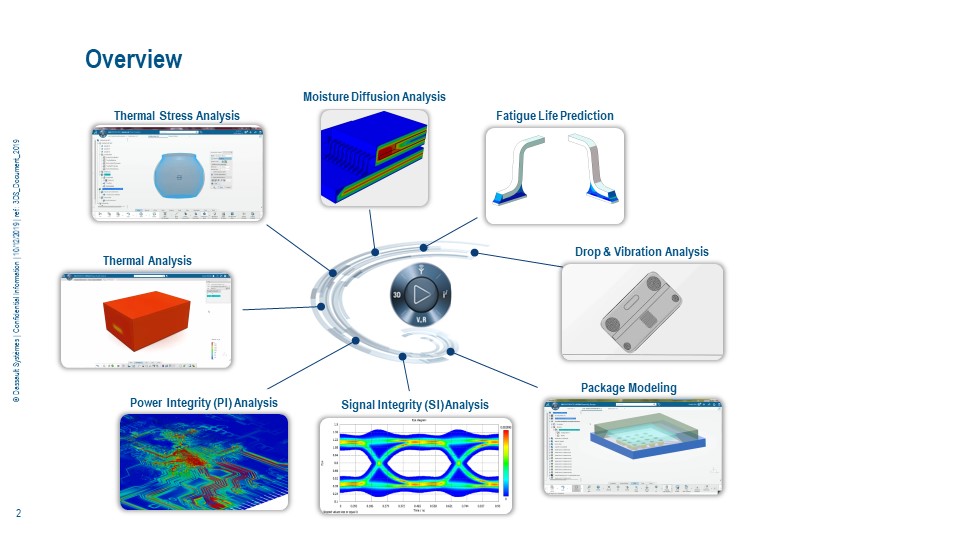
The solvers in the CST Studio Suite can be used for a wide range of electromagnetic, thermal and mechanical simulations. Applying them to package design and analysis allows designers fully understand each of the multi-disciplinary aspects of the package design. The integrated environment allows a DOE approach to specifying and verifying the package design to fully understand the performance tradeoffs.
Dassault Systèmes has also thought a lot about the user experience for engineers using the 3DEXPERIENCE platform. They offer advanced HPC capabilities and Cloud computing services for faster throughput and reduced simulation costs. Dassault Systèmes has built lightweight visualization technologies for viewing and sharing 3D models and simulation results in web-based apps.
Packaging can be make-or-break for many semiconductor products and systems. This is especially true when looking at product lifecycle management and reliability. It is one thing to design something that works when brand new, but over time residual stresses from operation and the environmental impact can lead to reduced fatigue life or even failure. In applications such as automotive, the expected lifetime of a product in the field should extend out decades, way beyond the expected lifetime of many consumer gadgets. The economic or even human cost of a failure can also be incredibly high.
The Dassault Systèmes website has detailed information on their solutions for advanced electronics packaging. For more information click HERE.
Also Read
A Brief History of IP Management
Delivering Innovation for Regulated Markets
Webinar: Next Generation Design Data & Release Management
Share this post via:


Consolidation and Competition: Who is Winning the $4.5 Billion Interface IP Race?