
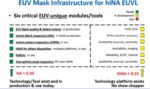
At the recent SPIE Advanced Lithography + Patterning Conference, Mark Phillips from Intel gave an insightful update on the status of the introduction of the 0.55 high numerical aperture extreme ultraviolet lithography technology. Mark went so far as to assert that the development progress toward high-NA EUV would support … Read More

Author: Tom Dillinger
0.55 High-NA Lithography Update
TSMC’s Reliability Ecosystem

TSMC has established a leadership position among silicon foundries, based on three foundational principles:
- breadth of technology support
- innovation in technology development
- collaboration with customers
Frequent SemiWiki readers have seen how these concepts have been applied to the fabrication and packaging technology… Read More
Self-Aligned Via Process Development for Beyond the 3nm Node
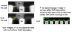
The further scaling of interconnect and via lithography for advanced nodes is challenged by the requirement to provide a process window that supports post-patterning critical dimension variations and mask overlay tolerances. At the recent international Electron Devices Meeting (IEDM) in San Francisco, TSMC presented … Read More
Technology Design Co-Optimization for STT-MRAM
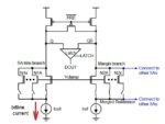
Previous SemiWiki articles have described the evolution of embedded non-volatile memory (eNVM) IP from (charge-based) eFlash technology to alternative (resistive) bitcell devices. (link, link)
The applications for eNVM are vast, and growing. For example, microcontrollers (MCUs) integrate non-volatile memory for … Read More
Advanced 2.5D/3D Packaging Roadmap
Frequent SemiWiki readers are no doubt familiar with the advances in packaging technology introduced over the past decade. At the recent International Electron Devices Meeting (IEDM) in San Francisco, TSMC gave an insightful presentation sharing their vision for packaging roadmap goals and challenges, to address the growing… Read More
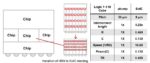
Heterogeneous Integration – A Cost Analysis
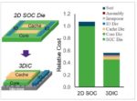
Heterogeneous integration (HI) is a general term used to represent the diverse possibilities for die technology incorporated into advanced 2.5D/3D packaging. At the recent International Electron Devices Meeting (IEDM) in San Francisco, a team from Synopsys and IC Knowledge presented data from analyses of future potential… Read More
Methodology for Aging-Aware Static Timing Analysis
At the recent Design Automation Conference, Cadence presented their methodology for incorporating performance degradation measures due to device aging into a static timing analysis flow. [1] (The work was a collaborative project with Samsung Electronics.) This article reviews the highlights of their presentation.
Background… Read More
Top 10 Takeaways from DAC 2021
The “in-person” portion of the Design Automation Conference (DAC) was recently held in San Francisco. (As several presenters were unable to attend, a “virtual” program is also available.) The presentations spanned a wide gamut – e.g., technical advanced in design automation algorithms; new features in commercial EDA tools; … Read More
Update on TSMC’s 3D Fabric Technology
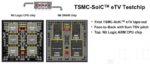
TSMC recently held their 10th annual Open Innovation Platform (OIP) Ecosystem Forum. An earlier article summarized the highlights of the keynote presentation from L.C. Lu, TSMC Fellow and Vice-President, Design and Technology Platform, entitled “TSMC and Its Ecosystem for Innovation” (link).
Overview of 3D Fabric
The TSMC… Read More
Design Technology Co-Optimization for TSMC’s N3HPC Process
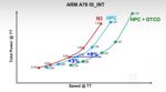
TSMC recently held their 10th annual Open Innovation Platform (OIP) Ecosystem Forum. An earlier article summarized the highlights of the keynote presentation from L.C. Lu, TSMC Fellow and Vice-President, Design and Technology Platform, entitled “TSMC and Its Ecosystem for Innovation” (link).
One of the topics that L.C. … Read More


TSMC CoWoS versus Intel EMIB Semiconductor Packaging