At the recent SPIE Advanced Lithography + Patterning Conference, Mark Phillips from Intel gave an insightful update on the status of the introduction of the 0.55 high numerical aperture extreme ultraviolet lithography technology. Mark went so far as to assert that the development progress toward high-NA EUV would support production deployment in 2025. This article summarizes the highlights of Mark’s presentation, including a forecast beyond the 0.55NA generation.
The high numerical aperture system with the 13.5nm wavelength source will enable the improved resolution required for sub-13nm half-pitch exposure, as well as greater image contrast for better printed line uniformity. (The resolution of an optical system is inversely proportional to the NA.) The resolution for high-NA EUV litho is often quoted as “13nm to 8nm half-pitch”.
Parenthetically, Mark described the transition to production high-NA lithography in 2025, as depicted in the ASML tool roadmap figure below. Intel has been actively collaborating with ASML, as will be discussed shortly. Yet, Mark did not cover topics that are commonly of interest to SemiWiki reads – e.g., a forecast for the number of high-NA EX:5000 systems to be released by ASML, the number of mask layers transitioning to 0.55NA, etc.

(The footnotes in the figure above next to system releases indicate that the initial wafer-per-hour specifications may start at a dose of 20mJ/cm**2 (250W), expanding to 30mJ/cm**2 (500W) in subsequent product updates.)
History
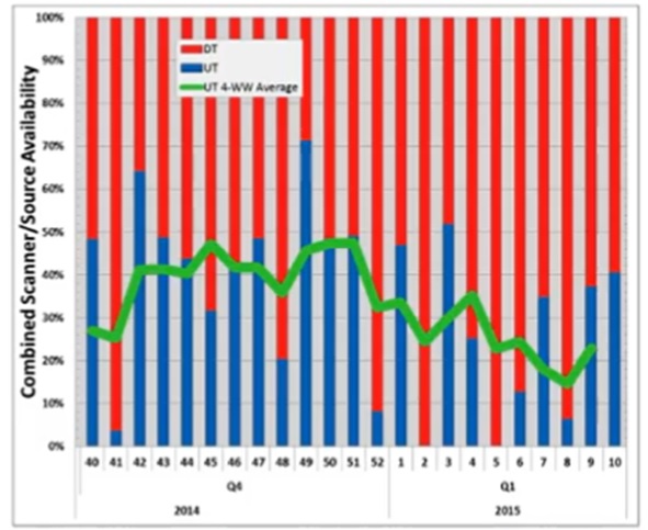
Mark began the presentation with a review of the introduction of the 0.33NA EUV technology. He recounted the difficulties in achieving target source power and availability in the development cycle for first-generation systems in the 2014-2017 timeframe. The figure below depicts the system uptime (blue), downtime (red), and 4-week rolling average (green) in the Q4 2014 to Q1 2015 interval.
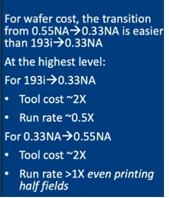
Wafer cost assessments reflected the increased tool cost, mask cost, and the throughput impact of the 0.33NA transition.
“Pitch division lithography (multi-patterning) at 193i was working well.”, Mark indicated. “The lithography infrastructure needed in conjunction with the EUV transition was not fully available. The compelling reason to move to 0.33NA EUV was the impact of pitch division on the edge placement error (EPE). The overlay alignment complexity with pitch division grew tremendously.” The figure below illustrates an example of the mask alignment dependencies to which Mark referred, as an increasing number of double-pattern mask layers were used.

Mark indicated that the transition to 0.55NA EUV will be easier from a cost analysis perspective, when addressing the replacement of a dual-patterned 0.33NA layer with a single 0.55NA mask, compared to the earlier cost tradeoff when replacing 193i masks with a single 0.33NA mask, as shown below. (More on “half-field printing” with 0.55NA shortly.)
EUV infrastructure
The discussion of EUV lithography tends to focus on the ASML scanners – yet, there is a rich and complex set of interdependent technologies that need to accompany any change in the exposure system:
- resists
- dose sensitivity, viscosity, coat uniformity vs. thickness, achievable resolution, and understanding of the photon/ion/electron interactions within the material upon exposure
- mask blank quality
- flatness, defects, coefficient of thermal expansion
- patterned mask quality
- defects, reflectivity/extinction of mask absorber layers
- mask defect inspection technology – resolution and throughput
- pellicles
- transmissivity, uniformity, compatibility with exposure to high energy illumination, post-pellicle attach defect inspection
Mark complimented the larger lithography industry on the corresponding progress made in all these areas, with specific mention of the inspection metrology system providers. He said, “By 2019, all of the infrastructure systems for 0.33NA EUV were ‘green’, although improvements are still needed in the transmission, uniformity, and power resiliency of pellicles.”
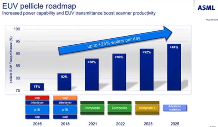
The chart below from ASML illustrates the direct relationship between the pellicle transmittance and wafer throughput, with a goal of “advanced pellicle materials” in 2025 providing >94% transmission.
0.55 High-NA Transition
Mark shared the goals of upcoming process node transitions:
-
- 7nm node: 18nm half-pitch
- 5nm node: 13nm HP
- 3nm node: 10nm HP
He then reviewed various facets of the 0.55NA infrastructure.
- EUV EXE:5000 System
“The confidence level in the availability of the next-generation EUV scanners is high. These systems leverage many of the existing sub-systems in the first generation NX:3000 series.”, Mark said.
The figure below illustrates the new sub-systems (in purple) for the high-NA EUV system, and the sub-systems ported from the current series.
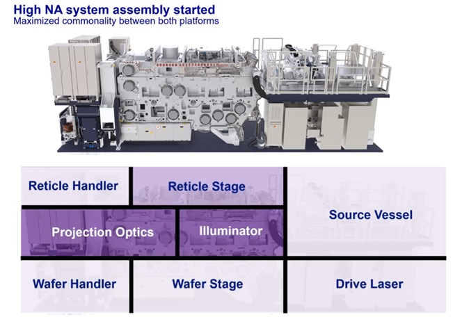
“The projection optics is a critical, new module, to be sure. The collaborative development between Zeiss and ASML is progressing well.”, Mark said. (The specifications for the Zeiss mirrors in the next-gen system are pretty amazing.)
As to the requisite EUV resists, Mark indicated that there is still active development on both chemically-amplified resists (CAR) and metal-oxide resists. “There are several optimization parameters still being evaluated, include the resist type, viscosity, thickness, and energy dose to achieve the target resolution, developed resist profile, and line edge uniformity.”, Mark indicated.
The figure below shows SEM and atomic force microscope profile results for a 0.55NA resist experiment, at 20nm spun thickness (using 0.33NA exposure).
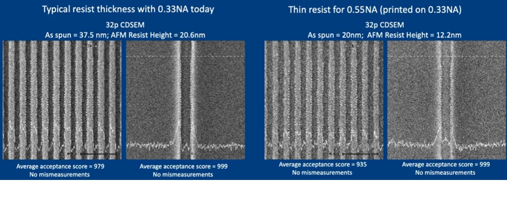
Mark noted that moving from a resist thickness of ~37.5nm for 0.33NA process steps to the much thinner layer for 0.55NA requires detailed attention to the resist viscosity and spin process steps. (The thinner resist maintains a 2:1 aspect ratio for the resist height to width. Note that the depth-of-field for exposure is reduced for higher NA optical systems, another consideration in the selection of the resist thickness. Also note that thinner resists result in reduced SEM image contrast, requiring continuing development for improved, high throughput resist metrology.)
- high-NA EUV masks
The 0.55NA systems have adopted a unique innovative optical path. The increase in the numerical aperture of the optical field necessitated a corresponding change in the mask-to-wafer reduction for exposure. The projection optics utilizes an anisotropic reduction factor – i.e., 4X reduction in the x-dimension and 8X in the y-dimension. (Mark credited ASML and Zeiss with the idea for this innovation.) Yet, as illustrated in the figure below, a traditional 6” mask dimension would not support a “full reticle” 26mm X 33mm field – the 8X demag y-range exceeds the mask height.
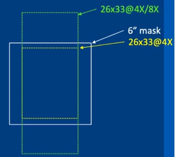
As a result, there will be a dual “half-field” mask exposure sequence for each high-NA EUV layer.
Mark indicated the remainder of the 0.55NA EUV mask infrastructure will be strongly leveraging the existing technologies developed for 0.33NA. As depicted in the figure below, there is “no show stopper” in the path to production.
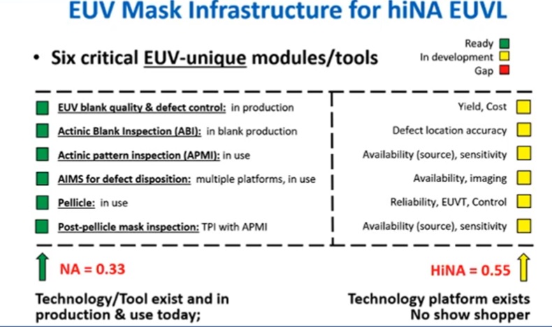
As an aside, Mark said, “The metrology challenges associated with the transition to (gate-all-around) RibbonFET devices far exceed those related to high-NA EUV mask inspection and measurement.”
Timeline to Production
In a separate talk at the SPIE Advanced Lithography conference, ASML and imec indicated they are setting up a high-NA EUV system prototype facility in Veldhoven, The Netherlands, to be on-line in 2023. The lab will allow further development of resist and methodology processes by the lab partners.
Mark indicated, “Intel will continue to partner closely with ASML, work with the high-NA researchers at this lab. We anticipate installing a pilot tool system in Oregon in late 2023 or early 2024, with production in 2025.”
The Future – 0.7NA Systems
Mark concluded his talk with a brief discussion on future high-NA development, for even greater resolution. (One could argue that the economic nature of Moore’s Law is under duress, but certainly not the lithographic characteristics.)
Mark posited that the next target could be:
- 7NA
- non-integer mask reduction optical path (e.g., 7.5X in the y-dimension, 5X in the x-dimension)
- the emergence of new mask materials and dimensions
Mark said, “We need a very low thermal expansion material (LTEM) for mask blanks. We will need better absorbers. And, we will need a new ‘standard’ mask size.” The figure below indicated how a 300mm round (775um thick substrate) could be applied.
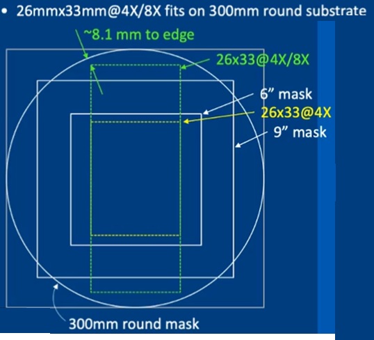
“Using a 300mm round mask would leverage a great deal of existing subsystem experience work with these dimensions.”, Mark suggested.
Summary
Intel is collaborating with ASML for early high-NA system availability in 2024, with a production date target in 2025. The confidence level in these dates is relatively high, due to the significant leverage of experience with 0.33NA, from re-use of scanner subsystems to major achievements in mask metrology and inspection technology.
Although significant development remains in the selection of resists and pellicles for high-NA exposure, the optical system in the new scanner is the critical path – “as it should be”, according to Mark.
The adoption of 0.55NA lithography will enable sub-13nm half-pitch critical dimensions, consistent with Intel’s process roadmap beyond the 18A node.
-chipguy
Also read:
Intel Best Practices for Formal Verification
Share this post via:


Comments
4 Replies to “0.55 High-NA Lithography Update”
You must register or log in to view/post comments.