
TSMC recently held their 10th annual Open Innovation Platform (OIP) Ecosystem forum. The talks included a technology and design enablement update from TSMC, as well as specific presentations from OIP partners on the results of recent collaborations with TSMC. This article summarizes the highlights of the TSMC keynote from… Read More

Author: Tom Dillinger
Highlights of the TSMC Open Innovation Platform Ecosystem Forum

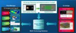
Design Planning and Optimization for 3D and 2.5D Packaging
Introduction
Frequent SemiWiki readers are aware of the growing significance of heterogeneous multi-die packaging technologies, offering a unique opportunity to optimize system-level architectures and implementations. The system performance, power dissipation, and area/volume (PPA/V) characteristics of a multi-die… Read More
Intel Architecture Day – Part 2: GPUs, IPUs, XeSS, OpenAPI

Introduction
At the recent Intel Architecture Day presentations, a breadth of roadmap plans were provided – an earlier article focused on the x86 client and data center cores and products. This article focuses on the GPU and IPU announcements.
Xe Graphics Core
The Intel GPU architecture for embedded, discrete, and data center… Read More
Intel Architecture Day – Part 1: CPUs

Introduction
The optimization of computing throughput, data security, power efficiency, and total cost of ownership is an effort that involves managing interdependencies between silicon and packaging technologies, architecture, and software. We often tend to focus on the technology, yet the architecture and software… Read More
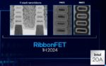
Highlights of the “Intel Accelerated” Roadmap Presentation
Introduction
Intel recently provided a detailed silicon process and advanced packaging technology roadmap presentation, entitled “Intel Accelerated”. The roadmap timeline extended out to 2024, with discussions of Intel client, data center, and GPU product releases, and especially, the underlying technologies to be … Read More
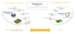
Ansys Multiphysics Platform
Background
Traditionally, the interface between chip designers and system power, packaging, reliability, and mechanical engineering teams was a relatively straightforward exchange of specifications. Chip designers developed preliminary power dissipation estimates, often based on a simplifying power/mm**2 value. … Read More
Magnetic Immunity for Embedded Magnetoresistive RAM (eMRAM)
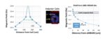
Previous SemiWiki articles have discussed the introduction of embedded Spin-Transfer Torque Magnetoresistive RAM IP from GLOBALFOUNDRIES, as an evolution replacement for non-volatile embedded flash memory. (link, link)
Those articles described the key features of STT-MRAM technology, but didn’t delve into a key reliability… Read More
EDA Flows for 3D Die Integration
Background
The emergence of 2.5D heterogeneous die integration using a silicon (or organic) interposer has enabled unique system architectures. The term “More than Moore” has been used to describe the circuit density and cost advantages of leveraging multiple die in the package, the die potentially in different process technologies. … Read More
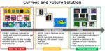
TSMC Design Considerations for Gate-All-Around (GAA) Technology
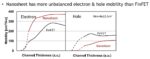
The annual VLSI Symposium provides unique insights into R&D innovations in both circuits and technology. Indeed, the papers presented are divided into two main tracks – Circuits and Technology. In addition, the symposium offers workshops, forums, and short courses, providing a breadth of additional information.
At… Read More
Resist Development for High-NA EUV
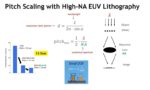
The successful transition to a new fabrication process from development to high volume manufacturing requires a collective, collaborative effort among process engineers, equipment manufacturers, and especially, chemical suppliers. Of particular importance is the chemistry of the photoresist materials and their interaction… Read More


TSMC CoWoS versus Intel EMIB Semiconductor Packaging