Previous SemiWiki articles have discussed the introduction of embedded Spin-Transfer Torque Magnetoresistive RAM IP from GLOBALFOUNDRIES, as an evolution replacement for non-volatile embedded flash memory. (link, link)
Those articles described the key features of STT-MRAM technology, but didn’t delve into a key reliability concern – namely, the degree of “immunity” of the MRAM bitcell array to external magnetic fields. These fields could disrupt the magnetic polarization of the bitcell, if the field magnitude was sufficient to overcome the coercivity of the magnetic materials used in the bitcell tunnel junction (MTJ).
Note that these magnetic fields could originate from sources applied outside the SoC package – e.g., from the earth’s magnetic field, or from a malicious attempt to perturb the non-volatile stored data. In addition, the MTJ will be exposed to magnetic fields originating with the package itself – e.g., from an inductive loop coil fabricated on the die, part of an LC-tank circuit used in an oscillator or SerDes IP macro. It is crucial to understand the magnetic immunity of an eMRAM IP array when exposed to fields from either of these sources.
There are two definitions of magnetic immunity, whether the array is in “standby” (SMI) or “active” (AMI) mode – active is the more critical.
At the recent 2021 VLSI Symposium, Vinayak Bharat Naik, MRAM lead at GLOBALFOUNDRIES, provided results of magnetic immunity experimental analysis for MRAM arrays fabricated in the 22FDX-SOI process technology.[1] Note that this technology also has very attractive RF device characteristics – thus, there may be on-die RF IP with inductive elements that emanate significant field magnitudes. The rest of this article highlights the insights in Vinayak’s presentation on MRAM magnetic immunity.
Background
Briefly, a STT-MRAM bitcell consists of three key material layers, commonly in a vertical configuration – i.e., a “perpendicular” magnetic tunnel junction (MTJ). The MTJ is comprised of: a “fixed” (or reference) magnetic polarization orientation material; a thin (tunnel) dielectric; and, a “free” magnetic material whose polarization can be switched by the write current direction through the MTJ bitcell. The write current needs to be of sufficient magnitude and duration.
After the write cycle, the resulting states of the bitcell are “parallel” (low read cycle series resistance) or “anti-parallel” (high read cycle series resistance), referring to the magnetic orientation of the two layers on either side of the tunnel junction, as illustrated below.

The figure above provides a comparison of the key features of the STT-MRAM bitcell, relative to embedded flash (to achieve suitably low PPM failure rates):
- endurance (# of read/write cycles)
- retention (non-volatile array storage)
- read/write cycle performance
- cost
All of these features need to apply over stringent environmental conditions – e.g., -40C to 125C – corresponding to the industrial applications for the SoC with the eMRAM IP.
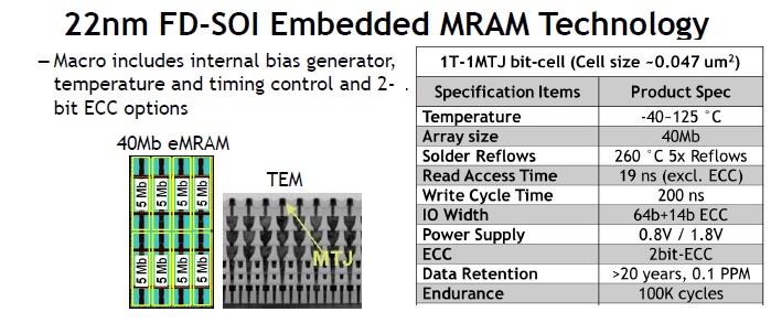
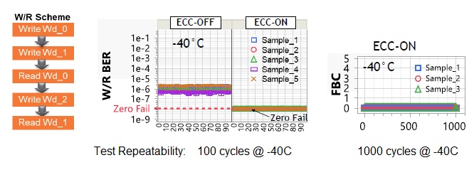
Vinayak provided the results of a stress test consisting of a large number of iterative write-read cycles applied to the 40Mb 22FDX MRAM array depicted above. (The temperature corner of -40C is the most critical.) With ECC applied to the memory data operations, using the data + ECC bits macro architecture shown above, all “raw” data errors were corrected – i.e., the bit error rate (BER) was reduced to zero.
The MTJ is fabricated as part of the BEOL fabrication process steps, as shown in the TEM cross-section above. The high-temperature FEOL steps have been completed. Yet, it is imperative that the MTJ functionality is not impacted by subsequent exposure to elevated temperatures, such as solder reflow for die attach. Vinayak also shared data that showed no increase in the BER after 5 reflow cycles of 260C (e.g., 40-80 seconds above 220C).
Magnetic Immunity to External Fields
As the basis for the non-volatile MTG states is the coercivity of the materials to an external magnetic field, the magnetic immunity (MI) of the STT-MRAM array is a new reliability parameter, not applicable to embedded flash.
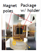
As mentioned above, the external field could originate from outside the SoC package. Vinayak showed the experimental setup and MI analysis results applied to an STT-MRAM testsite. The figures below show the test fixture and illustrate that the (ECC-corrected) memory write-read BER was zero, with an active MI greater than 250 Oe.
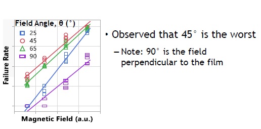
Parenthetically, Vinayak also highlighted that the anisotropic nature of the magnetization domains within the MTJ layers suggests that the angle of incidence between the external magnetic field and the STT-MRAM testsite surface could affect the coercivity. The figure below confirms this effect, as an angle of 45degrees between field and surface had the lowest MI.
Also, Vinayak noted that the MI will increase for smaller diameter MTJ bitcells, ensuring that STT-MRAM technology will continue to be attractive with subsequent process scaling.
For reference, here are some representative values of magnetic intensity, to compare to the MI target of >250 Oe:
- earth’s magnetic field: 5 Oe
- refrigerator magnet: 50 Oe
- electromagnet in a junkyard for lifting cars: ~10,000 Oe
- clinical MRI scanner: ~5,000 – 30,000 Oe
Vinayak briefly described the importance of integrating a “magnetic shield” material into the SoC package for embedded STT-MRAM IP, where exposure to high magnetic fields may be a concern. For several years, GLOBALFOUNDRIES has had a strong collaboration with Everspin Technologies on MRAM development. Everspin is shipping stand-alone MRAM parts. “All Everspin products contain embedded magnetic shielding within their packages.” [2]
(For additional information on the types of shielding materials used and the degree of magnetic isolation provided, check out reference [3].)
On-Die Magnetic Immunity
There are two facets to magnetic immunity within the SoC die:
- fields originating from an inductive coil, such as used in an LC tank circuit, contributing to STT-MRAM error rates
- fields originating from the MTJ array itself, impacting the LC tank functionality
Vinayak shared analysis data showing the magnetic field strength from an inductive coil as a function of separation distance, as shown below.
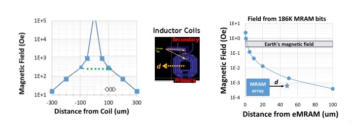
For the model shown, a separation distance between a coil and MTJ array greater than 100um was sufficient to ensure the fields from the coil are below the target MI. (A typical SoC design will likely contain multiple LC tank circuits, necessitating design-specific model analysis.)
The graph on the right above shows the magnetic field originating from an embedded STT-MRAM array, as a function of distance. In the example above, the MRAM array field is very small, and thus would have negligible impact on the LC tank oscillation frequency.
Summary
Embedded STT-MRAM IP is emerging as a non-volatile storage replacement for eFlash at advanced process nodes, as exemplified by the offering from GLOBALFOUNDRIES in their 22FDX-SOI technology. The performance, endurance, retention, and cost of STT-MRAM are extremely attractive. (Architecturally, ECC bits added to the data word are required to achieve a zero bit error rate.)
The eMRAM does introduce a new reliability concern – the “magnetic immunity” of the array to external magnetic fields, either from outside the SoC package or from inductive circuits on the die. The package composition may need additional magnetic shielding, if the potential field magnitude could exceed the MI. For on-die inductors, suitable spacing to the eMRAM array will ensure the MI reliability limits are not exceeded.
I would encourage you to review the MI analysis techniques and results that GLOBALFOUNDRIES presented at the 2021 VLSI Symposium. Also, here is a link to an informative GLOBALFOUNDRIES webinar on embedded NVM IP development – link.
-chipguy
References
[1] Vinayak Bharat Naik, “STT-MRAM: A Robust Embedded Non-Volatile Memory with Superior Reliability and Immunity to External Magnetic Field and RF Sources”, VLSI Symposium, 2021, paper T12-2.
[2] Everspin Technologies, “Magnetic Field Immunity of Everspin MRAM”, whitepaper EST02880, www.everspin.com/file/784/download .
[3] https://magneticshields.co.uk/technical/magnetic-shielding-how-does-it-work
Also Read:
GloFo inside Intel? Foundry Foothold and Fixerupper- Good Synergies
Silicon Photonics Solutions Address Bandwidth, Reach, and Power Challenges
Enabling Silicon Technologies to Address Automotive Radar Trends and Requirements
Share this post via:


Is Intel About to Take Flight?