Summary
A novel spin-transfer torque magnetoresistive memory (STT-MRAM) IP offering provides an attractive alternative for demanding high-performance embedded applications.
Introduction
There is a strong need for embedded non-volatile memory IP across a wide range of applications, as depicted in the figure below.
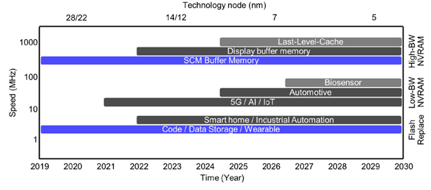
The future scaling of embedded non-volatile flash memory IP is ineffective at more advanced nodes. Several alternative memory technologies have been pursued as a “flash replacement” – e.g., phase change memory (PCM) materials, resistive change memory (RRAM), spin-transfer torque magnetoresistive memory (STT-MRAM). These technologies offer dense bit cells (“1T1R”) and operate by changing the static electrical resistance of the cell as a result of the “Write1” and “Write0” pulse current and magnitude through the material. A read operation senses the resistance magnitude when the cell is accessed, with much reduced cell current. The ratio between the two resistances is ideally very high, to accelerate the read operation.
As a replacement for embedded flash, these technologies are evaluated against a number of criteria:
- Non-volatility measures – i.e., operating temperature range, data retention (very temperature-dependent)
- Bit density
- Bit cell resistance ratio
- Write access time, read access time
- Array write granularity
- Low power
- Endurance (reflected as the # of R/W cycles before a bit error rate threshold is exceeded)
- Additional fabrication complexity (i.e., cost)
The embedded memory technology that has the fastest adoption rate is currently STT-MRAM. A cross-section of the “magnetic tunnel junction” (MTJ) of the bit cell is illustrated below. The cell consists of two ferromagnetic layers separated by a thin tunnel oxide. The magnetic polarization of the “free layer” is altered by the direction and magnitude of the write current. The electrical resistance through the layers differs greatly, whether the free layer polarization is “parallel” or “anti-parallel” to the reference layer. Previous semiwiki articles have described the operation of the STT-MRAM in detail. [ Refs. 1, 2]
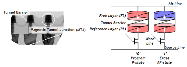
The magnetic and electron tunnel layers for the STT-MRAM are readily fabricated and lithographically patterned. The MTJ satisfies the typical embedded flash requirements, as listed in the first figure, with the great benefit of highly granular addressability.
For the set of embedded memory applications listed above demanding very high performance and endurance, these attractive characteristics of STT-MRAM technology will require ongoing R&D investment.
STT-MRAM for High Performance and Endurance
At the recent VLSI 2020 Symposium, a team from GLOBALFOUNDRIES introduced a novel high-performance STT-MRAM offering. [3] A new MTJ material layer stack was developed, to optimize the read access time and concurrently (and significantly) extend the number of endurance cycles. (Additional process engineering focus was also given to tighter CD lithography.)
The overall specifications for this new STT-MRAM IP are given in the table below:
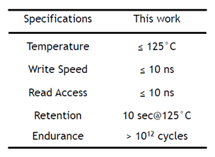
Note that the endurance target for high-performance applications is defined using a bit error rate (BER) limit of 1E-06 (1 ppm) with a 10nsec write pulse.
The engineering tradeoff for this high-performance offering is that the retention property is reduced to 10sec @ 125 degrees C, as the MTJ energy barrier for this new high-performance cell is much lower compared to an eFlash-like replacement design. (The retention of 10sec @ 125C equates to ~1 week @ 85C.) This will necessitate a low-overhead refresh cycle.
A couple of interesting engineering optimizations were added to the array implementation by the GLOBALFOUNDRIES team:
- An adaptive operating voltage is applied to the MTJ array.
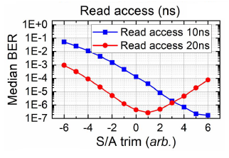
- The read sense amplifier is “trimmed” for optimal performance.
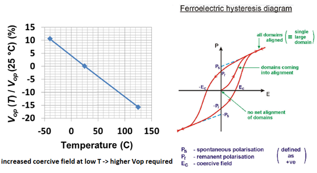
For example, the voltage bias for both the Write1 and Write0 current directions is adapted to respond to an internal temperature sensor. The required Vop is higher at lower temperature – e.g., +10% at -40C (and -16% at 125C) compared to 25C. This is due to the higher “coercive” magnetic field at low temperature that has to be overcome to alter the polarization.
The following figures highlight the technology qualification data that GLOBALFOUNDRIES presented at the symposium.
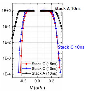
The first figure shows the median BER for two different MTJ material stacks with different write pulse widths, as a function of Vop. Stack “C” was optimized for a single write pulse of 10nsec. (Note that longer current pulses and/or multiple pulses, potentially including an intermediate read-verify operation, improves the BER.)
The figure below illustrates the BER for a read access cycle for stack “C” at 125C, with sense amp trimming.
STT-MRAM Reliability
Reliability evaluations were undertaken to ensure no adjacent bit cell “disturb” fails.
The endurance specification for the STT-MRAM array required development of an MTJ lifetime model, using BER data taken at accelerated voltage and temperature conditions. (The time required to exercise sufficient array data would be prohibitive, necessitating the accelerated stress technique commonly used for other failure mechanism models.) The GLOBALFOUNDRIES team noted that there is extensive model history for the time-dependent dielectric breakdown (TDDB) of conventional device gate oxides, but as yet, little modeling history of MTJ lifetime breakdown mechanisms.
The result of the endurance data (for 1ppm BER) is the reliability model illustrated below:
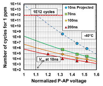
The figure illustrates the model extrapolation to >1E12 endurance cycles at -40C, using the most aggressive write cycle pulse of 10nsec. For higher temperatures than -40C (lower Vop) and greater write pulse widths, the number of endurance cycles for this optimized MTJ stack will be much greater.
With extensive R&D engineering, the GLOBALFOUNDRIES team has demonstrated a novel MTJ materials stack, providing a “high performance” variants of an STT-MRAM array. Whereas the initial IP offerings of this technology provide an attractive replacement for non-volatile eFlash, this new technology pushes STT-MRAM into an extremely competitive position for the NVRAM applications described in the opening figure.
For more info on the STT-MRAM technology from GLOBALFOUNDRIES, please follow this link.
-chipguy
References
[3] Lee, T.Y., et al., “Fast Switching of STT-MRAM to Realize High Speed Applications”, VLSI 2020 Symposium, paper TM3.3.
[4[ Naik, V. “A Reliable TDDB Lifetime Projection Model Verified Using 40Mb STT-MRAM Macro at Sub-ppm Failure Rate to Realize Unlimited Endurance for Cache Applications”, VLSI 2020 Symposium, paper TM3.4.
Images supplied by the VLSI Symposium on Technology & Circuits 2020.
Also Read:
Webinar on eNVM Choices at 28nm and below by Globalfoundries
GLOBALFOUNDRIES Sets a New Bar for Advanced Non-Volatile Memory Technology
Specialized Accelerators Needed for Cloud Based ML Training
Share this post via:


Solving the EDA tool fragmentation crisis