Whether it’s the solid-state disk in your laptop, IoT/automotive hardware or edge-based AI, embedded non-volatile memory (eNVM) is a critical building block for these and many other applications. The workhorse technology for this capability has typically been NOR flash (eFlash), but a problem looms as eFlash presents challenges to scale economically below the 28nm node. That’s why a recent press release from GLOBALFOUNDRIES (GF) caught my attention:
Embedded magnetoresistive non-volatile memory (eMRAM) is a mouthful. I did a bit of research, and MRAM was presented back in 1974, when IBM developed a component called a Magnetic Tunnel Junction (MTJ). The device had two ferromagnetic layers separated by a thin insulating layer and a memory cell was created by the intersection of two wires (i.e., a row line and a column line) with an MJT between them. MRAMs can combine the high speed of SRAM, the storage capacity of DRAM, and the nonvolatility of eFlash at low power, so a production embedded implementation of the technology below 28nm is a big deal.
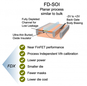
First, a bit about the implementation technology. 22FDX is a 22nm fully 
depleted silicon-on-insulator (FD-SOI) technology from GF. Another mouthful. FD-SOI delivers near FinFET-like performance without the design and manufacturing complexities of FinFET. The figure at the right summarizes the benefits of GF’s 22FDX.
“We continue our commitment to differentiate our FDX platform with robust, feature rich solutions that allow our clients to build innovative products for high performance and low power applications,” said Mike Hogan, senior vice president and general manager of Automotive and Industrial Multi-market at GLOBALFOUNDRIES. “Our differentiated eMRAM, deployed on the industry’s most advanced FDX platform, delivers a unique combination of high performance RF, low power logic and integrated power management in an easy-to-integrate eMRAM solution that enables our clients to deliver a new generation of ultra-low power MCUs and connected IoT applications.”
I caught up with Martin Mason, senior director automotive, industrial and multi
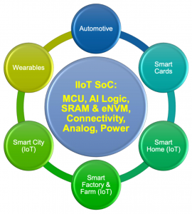
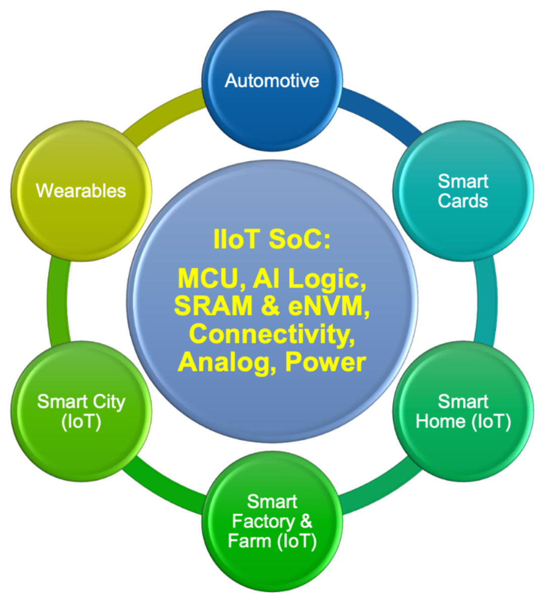
market BU at GF to get a bit more detail about their new, production-ready eMRAM. He took me through a very robust qualification process for the device, including a bit error rate in the 6E-6 range, robust data retention after 5X solder reflows, stand-by data retention sufficient for industrial-grade and automotive-grade 2 applications and multiple magnetic immunity tests. Martin summed up our discussion like this, “22FDX with embedded MRAM is an enabling technology platform for Intelligent IoT (IIoT), wearables, MCUs and advanced automotive products. We have a qualified Flash-like robust eMRAM process with our first client single product MRAM tape out in fab, multiple
clients running MRAM test chips and many silicon validated MRAM macros
(4Mb-48Mb). Unlike other eMRAM solutions we built GFs 22FDX MRAM to be  very robust with -40C to 125C operating range, high endurance and long data
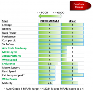
retention, passing five rigorous real-world (5x) solder reflow tests while maintaining leading magnetic immunity. The GF eMRAM is very much like eFLASH – only better, with faster read and write times and reduced mask count manufacturing compared with traditional embedded Flash technologies.” The diagram to the right summarizes GF’s new eMRAM vs. eFlash.
GF reports they are working with several clients with multiple production tape-outs scheduled in 2020 using the new, production-ready eMRAM technology in 22FDX. GF’s state-of-the-art 300mm production line at Fab 1 in Dresden, Germany will support volume production for these projects. They also report custom design kits featuring drop-in, silicon validated MRAM macros ranging from 4 to 48 mega-bits, along with the option of MRAM built-in-self-test support is available today from GF and their design partners.
Looking ahead, GF expects its scalable eMRAM to be available on both FinFET and future FDX platforms as a part of the company’s advanced eNVM roadmap. If you need an eFlash alternative below 28nm this is definitely something to look into.
Also Read:
Specialized Accelerators Needed for Cloud Based ML Training
The GlobalFoundries IPO March Continues
Magnetic Immunity for Embedded Magnetoresistive RAM (eMRAM)
Share this post via:


Solving the EDA tool fragmentation crisis