The rapid evolution of automotive technology has intensified the demand for highly reliable, high-performance semiconductor memory solutions. Modern vehicles increasingly rely ADAS driving features, and complex infotainment platforms, all of which require memory that can operate flawlessly under extreme environmental… Read More

Tag: stt-mram
Advancements in 3D Stacked IGZO 2T0C DRAM for Computing-in-Memory Applications
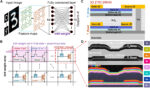
In the rapidly evolving field of artificial intelligence (AI), the demand for efficient data processing has exposed limitations in traditional memory technologies. The paper “3D Stacked IGZO 2T0C DRAM Array with Multibit Capability for Computing in Memory Applications,” published in Science Advances on May… Read More
2024 Outlook with Srinivasa Kakumanu of MosChip

MosChip is a publicly traded company founded in the year 1999, they offer semiconductor design services, turnkey ASIC, software services, and end-to-end product engineering solutions. The company headquartered in Hyderabad, India, with five design centers and over 1300 engineers located in Silicon Valley (USA), Hyderabad,… Read More
Technology Design Co-Optimization for STT-MRAM
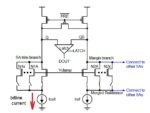
Previous SemiWiki articles have described the evolution of embedded non-volatile memory (eNVM) IP from (charge-based) eFlash technology to alternative (resistive) bitcell devices. (link, link)
The applications for eNVM are vast, and growing. For example, microcontrollers (MCUs) integrate non-volatile memory for … Read More
MRAM Magnetic Immunity – Empirical Study Summary
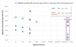
The main threat for the wide adoption of MRAM memories continues to be their lack of immunity to magnetic fields. MRAM magnetic immunity (MI) levels has seen significant research over the years and new data is continuously published from the main MRAM vendors.
This data, however, is rarely compared to magnetic field exposure scenarios… Read More
Embedded MRAM for High-Performance Applications
Summary
A novel spin-transfer torque magnetoresistive memory (STT-MRAM) IP offering provides an attractive alternative for demanding high-performance embedded applications.
Introduction
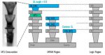
There is a strong need for embedded non-volatile memory IP across a wide range of applications, as depicted in the figure below.
The… Read More
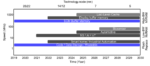
TSMC 32Mb Embedded STT-MRAM at ISSCC2020
32Mb Embedded STT-MRAM in ULL 22nm CMOS Achieves 10ns Read Speed, 1M Cycle Write Endurance, 10 Years Retention at 150C and High Immunity to Magnetic Field Interference presented at ISSCC2020
1. Motivation for STT-MRAM in Ultra-Low-Leakage 22nm Process
TSMC’s embedded Spin-Torque Transfer Magnetic Random Access Memory (STT-MRAM)… Read More
My Top Three Reasons to Attend IEDM 2019

The International Electron Devices Meeting is a premier event to learn about the latest in semiconductor process technology. Held every year in early December is San Francisco this years conference will be held from Decembers 7th through December 11th. You can learn more about the conference at their web site here.
This is a must… Read More
TechInsights Gives Memory Update at IEDM18 DRAM and Emerging Memories
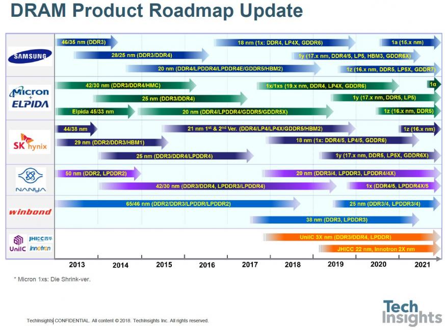
On the Sunday evening at IEDM last year, TechInsights held a reception in which Arabinda Das and Jeongdong Choe gave presentations that attracted a roomful of conference attendees.
This is the second part of the review of Jeongdong’s talk, we covered NAND flash technology in the last post. Jeongdong is a Senior Technical… Read More
STT-MRAM – Coming soon to an SoC near you
An increasing percentage of SoC die area is being allocated to memory arrays, as applications require more data/instruction storage and boot firmware. Indeed, foundries invest considerable R&D resources into optimizing their array technology IP offerings, often with more aggressive device features than used for other… Read More