
32Mb Embedded STT-MRAM in ULL 22nm CMOS Achieves 10ns Read Speed, 1M Cycle Write Endurance, 10 Years Retention at 150C and High Immunity to Magnetic Field Interference presented at ISSCC2020
1. Motivation for STT-MRAM in Ultra-Low-Leakage 22nm Process
TSMC’s embedded Spin-Torque Transfer Magnetic Random Access Memory (STT-MRAM) offers significant advantages compared to Flash Non-Volatile Memory (NVM). Flash requires 12 or more extra masks, is implemented in the silicon substrate and is page mode write alterable. STT-MRAM on the other hand is implemented in the Back-End-Of-Line (BEOL) metallization as shown in Fig. 1, requires only 2-5 extra masks and is byte-alterable.
This implementation in TSMC’s 22nm Ultra-Low-Leakage (ULL) CMOS process has a very high read speed of 10ns, and read power of 0.8mA/MHz-bit. It has 100K cycle write endurance for 32Mb code and 1M cycle endurance for 1Mb data. It supports data retention for IR reflow at 260C of 90 seconds and 10 years data retention at 150C. It is implemented in a very small 1transistor-1resistor (1T1R) 0.046 mm2 bit cell and has a very low leakage current of 55mA at 25C for the 32Mb array equivalent to 1.7E-12A/bit when in Low Power Standby Mode (LPSM). It utilizes a sensing scheme with per-sense amp trimming and 1T4R reference cell.

Fig. 1. Cross-section of the STT-MRAM bit cell in BEOL metallization layers between M1 and M5.
2. 1Transistor-1Resistor MRAM Bit Cell Operation and Array Structure
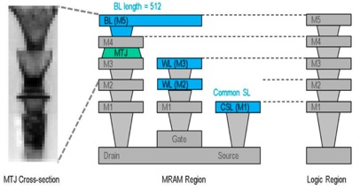
To reduce parasitic resistance on the write current path, a two-column common source line (CSL) array structure is employed as shown.

Fig. 2. Schematic of the 1T1R bit cell in the array of 512b column with the 2-column CSL
The word line is over-driven by a charge pump to provide sufficient switching current of hundred’s of mA for write operation requiring the unselected bit lines to be biased at a “write-inhibit voltage” (VINHIBIT) to prevent excess voltage stress on the access transistors of the unselected columns of the selected row. To reduce bit line leakage of the access transistor on unselected word lines, the word line has a negative voltage bias (VNEG). The biasing of the array structure for reading, write-0 and write-1 is shown in Fig. 3.

Fig. 3. Cell array structure biasing for word lines and bit lines for read, write-0 and write-1 operations.
3. Read Operation, Sense Amplifier and Word-Line Voltage System
For fast, low-energy wake-up from LPSM to enable high-speed read access, a fine-grained power gating circuit (one per 128 rows) with a two-step wakeup is used as shown in Fig. 4. The power switch consists of two switches, one for the chip power supply VDD and the other for a regulated voltage from the Low Drop-Out (LDO) regulator supplying VREG. The VDD switch is turned on first to pre-charge the WL driver’s power rail, then the VREG switch is turned on to raise the level to the targeted level, which achieves fast wake-up of <100ns while minimizing the transient current from VREG LDO.

Fig. 4. Fine-grained power gating circuit (one per 128 rows) with two-step wake-up.
The Tunnel Magnetoresistance Ratio (TMR) house curve shown in Fig. 5 is the ratio between the antiparallel resistance state Rap to the parallel resistance state Rp as a function of voltage, showing lower TMR and smaller read window at higher temperatures.

Fig. 5 House curve of TMR showing the reduced window for read at 125C
The resistance distributions of the Rap and the Rp states which, when including the bitline metal resistance and the access transistor resistance, determine the total read-path resistance showing the proportional reduction in the difference between the two states which the sense amp needs to measure to determine the bit value, as shown in Fig. 6.

Fig. 6. Distribution of resistance values for the anti-parallel Rap and the parallel Rp states and including the metal bit line and access transistor resistances showing the proportional reduction in the difference between the two states that needs to be detected by the sense amp.
To sense the resistance of the MTJ, the voltage across it during read must be clamped by transistors N1 and N2 to a low value to avoid read-disturb and is trimmed to cancel the sense amp and reference current offset. The reference resistance is formed by the 1T4R configuration R~(Rp +Rap)/2 + R1T as shown in Fig. 7.

Fig. 7. Sense amp with trimming capability showing the read clamp voltage on transistors N1 and N2 to prevent read disturb. Reference R~(Rp +Rap)/2 + R1T
This configuration is able to achieve a read speed of less than 10ns at 125C as shown in the sensing timing diagram and shmoo plot Fig. 8.

Fig. 8. Sensing timing diagram and read access shmoo plot at 125C.
4. MRAM write operation
MRAM write of the parallel low resistance state, Rp and the higher resistance anti-parallel state Rap requires bi-directional write operation shown in Fig. 9. To write the Rap state to the Rp requires biasing the Bl to VPP, the WL to VREG_W0 and the SL to 0 to write the 0 state. To write the 1 state, writing the Rp state to the Rap state requires current in the other direction, with the BL at 0, the SL at VPP and the WL at VREG_W1.

Fig. 9. Bi-directional Write for the parallel low resistance state, Rp and the higher resistance anti-parallel state Rap
For data retention during IR reflow at 260C for 90sec, an MTJ with a high energy barrier Eb is needed. This requires an increase in the MTJ switching current to hundreds of mA needed for reliable writing. The write voltage is temperature compensated and a charge pump generates a positive voltage for selected cells and a negative voltage for unselected word lines to suppress bit line leakage at high temperatures. The write voltage system is shown in Fig. 10.

Fig. 10 Showing the over-drive of the WL and BL/SL by the charge pump and the temperature compensated write bias
Temperature compensation for write voltage is required for operation with a wide temperature range. The write voltage shmoos from -40C to 125C are shown in Fig. 11 where the F/P blocks show fail at -40C while passing at 125C.

Fig. 11. Showing requirement for temperature compensation during write.
A BIST module with standard JTAG interface implements self-repair and self-trimming to facilitate test flow. The memory controller TMC implementing the Double Error Correction ECC (DECECC) shown in Fig. 12.

Fig. 12. BIST and Controller for self-repair and self-trimming during test and implementing DECECC.
The TMC implements the smart write algorithm which implements bias setup and verify/retry time for high write endurance (>1M cycles). It contains read-before-write to decide which bits need to be written and dynamic group-write to improve write throughput, multi-pulse write with write verify and optimizes write voltage for high endurance. The algorithm is shown in Fig. 13.

Fig. 13. Smart write algorithm showing dynamic group write and multi-pulse write with write verify.
5. Reliability Data, Key Features and Die Photo

Fig. 14. The write endurance test shows that the 32Mb chip access times and the read currents are stable before and after 100K -40C write cycles.

Fig. 15. The write endurance bit error rate is less than 1 ppm at -40C after 1M cycles.

Fig. 16. The increased thermal stability barrier Eb governing temperature dependence of data retention shows more than 10 years data retention at 150C, 1ppm.
Magnetic field interference is a potential concern in many applications for spin-based STT-MRAM. The solution is a 0.3mm thick magnetic shield deposited on the package as shown in Fig. 16 showing that in a field strength of 3500Oe of a commercial wireless charger for mobile devices the bit error rate of 100 hour exposure can be reduced from >1E6ppm to ~1ppm. Also, more than 10 years of data retention at 125C was shown at a magnetic field of 650 Oe.

Fig. 17. Sensitivity to a magnetic field of 3500 Oe reduced by a factor of 1E6.
Conclusions
The 22nm ULL 32Mb high-density MRAM has very low power, high read speed, very high data retention and endurance suitable for a wide range of applications. With a cell size of only 0.0456mm 2 , it has a read speed of 10ns and a read power of 0.8 mA/MHz/b and in low-power standby mode (LPSB) it has leakage less than 55mA at 25C, equivalent to 1.7 E-12 A/bit leakage. For 32Mb code, it has an endurance of 100K cycles and for 1Mb data >1M cycles. It has a capability of 90sec data retention under IR reflow at 260C and a long-term retention of > 10 years at 150C. The product spec is shown in Fig. 18 and die photo in Fig. 19.

Fig. 18. Summary table of N22 MRAM specification and die photo.

Fig. 19. 32Mb high-density MRAM macro in the 22nm Ultra-Low-Leakage CMOS process.
Share this post via:


Comments
5 Replies to “TSMC 32Mb Embedded STT-MRAM at ISSCC2020”
You must register or log in to view/post comments.