
Resistive RAM (ReRAM) technology has emerged as an attractive alternative to embedded flash memory storage at advanced nodes. Indeed, multiple foundries are offering ReRAM IP arrays at 40nm nodes, and below.
ReRAM has very attractive characteristics, with one significant limitation:
- nonvolatile
- long retention time
- extremely dense (e.g., 2x-4x density of SRAM)
- good write cycle performance (relative to eFlash)
- good read performance
but with
- limited endurance (limited number of ‘1’/’0’ write cycles)
These characteristics imply that ReRAM is well-suited for the emerging interest in compute-in-memory architectures, specifically for the multiply-accumulate (MAC) computations that dominate the energy dissipation in neural networks.
To implement a trained NN for inference applications, node weights in the network would be written to the ReRAM array, and the data inputs would be (spatially or temporally) decoded as the word lines accessing the array weight bits. The multiplicative product of the data/wordline = ‘1’ and the stored weight_bit = ‘1’ would result in significant memory bitline current that could be readily sensed to denote the bit product output – see the figure below.

At the recent International Solid State Circuits Conference (ISSCC), researchers from Georgia Tech University and TSMC presented results from an experimental compute-in-memory design using TSMC’s 40nm ReRAM macro IP. [1] Their design incorporates several unique features – this article summarizes some of the highlight of their presentation.
Background
As the name implies, ReRAM technology is based on the transitions of a thin film material between a high-resistance and low-resistance state. Although there are a large number of different types of materials (and programming sequences) used, a typical metal-oxide thin-film implementation is depicted in the figure below.

The metal oxide thin film material shown incorporates the source and transport of oxygen ions/vacancies under an applied electric field of high magnitude. (The researchers didn’t elaborate on the process technology in detail, but previous TSMC research publications on ReRAM development did utilize a TiO-based thin film programming layer. Multiple metal-oxide thin film materials are also used.)
As depicted in the figure above, an initial “filament forming” cycle is applied, resulting in transport of oxygen ions in the thin film. In the Reset state (‘0’), a high electrical resistance through the metal-oxide film is present. During the application of a Set (‘1’) write cycle, oxygen ion migration occurs, resulting in an extension of the filament throughout the thin film layer, and a corresponding low electrical resistance. In the (bipolar operation) technology example depicted above, the write_0 reset cycle breaks this filament, returning the ReRAM cell to its high resistance state.
The applied electric field across the top thin film for the (set/reset) write operation is of necessity quite large; the applied “read” voltage to sense the (low or high) bitcell resistance utilizes a much smaller electric field.
There are several items of note about ReRAM technology:
- the bitcell current is not a strong function of the cell area
The filamentary nature of the conducting path implies that the cell current is not strongly dependent on the cell area, offering opportunities for continued process node scaling.
- endurance limits
There is effectively a “wearout” mechanism in the thin film for the transition between states – ReRAM array specifications include an endurance limits on the number of write cycles (e.g., 10**4 – 10**6). Commonly, there is no limit on the number of read cycles.
The endurance constraints preclude the use of ReRAM as a general-purpose embedded “SRAM-like” storage array, but it is the evolutionary approach adopted as an eFlash replacement, and a compute-in-memory offering where pre-calculated weights are written, and updated very infrequently.
- resistance ratio, programming with multiple write cycles
The goal of ReRAM technology is to provide a very high ratio of the high resistance to low resistance states (HRS/LRS). When the cell is being accessed during a read cycle – i.e., data/wordline = ‘1’ – the bitline sensing circuit is simplified if i_HRS << i_LRS.
Additionally, it is common to implement a write to the bitcell using multiple iterations of a write-read sequence, to ensure the resulting HRS or LRS cell resistance is within the read operation tolerances. (Multiple write cycles are also initially used during the forming step.)
- HRS drift, strongly temperature dependent
The high-resistance state is the result of the absence of a conducting filament in the top thin film, after the oxygen ion transport during a write ‘0’ operation. Note in the figure above the depiction of a high oxygen vacancy concentration in the bottom metal oxide film. Any time a significant material concentration gradient is present, diffusivity of this material may occur, accelerated at higher temperatures. As a result, the HRS resistance will drift lower over extended operation (at high temperature).
Georgia Tech/TSMC ReRAM Compute-in-Memory Features
The researchers developed a ReRAM-based macro IP for a neural network application, with the ReRAM array itself providing the MAC operations for a network node, and supporting circuitry providing the analog-to-digital conversion and the remaining shift-and-add logic functionality. The overall implementation also incorporated three specific features to address ReRAM technology issues associated with: HRS and LRS variation; low (HRS/LRS) ratio; and, HRS drift.
low HRS/LRS ratio
One method for measuring the sum of the data inputs to the node multiplied times a weight bit is to sense the resulting bitline current drawn by the cells whose data/wordline = ‘1’. (Note that unlike a conventional SRAM block with a single active decoded address wordline, the ReRAM compute-in-memory approach will have an active wordline for each data input to the network node whose value is ‘1’. This necessitates considerable additional focus on read-disturb noise on adjacent, unselected rows or the array.) However, for a low HRS/LRS ratio, the bitline current contribution from cells where data = ‘1’ and weight = ‘0’ needs to be considered. For example, if (HRS/LRS) = 8, the cumulative bitline current of eight (data = ‘1’ X weight = ‘0’) products will be equivalent to one LRS current (‘1’ X ‘1’), a binary multiplication error.
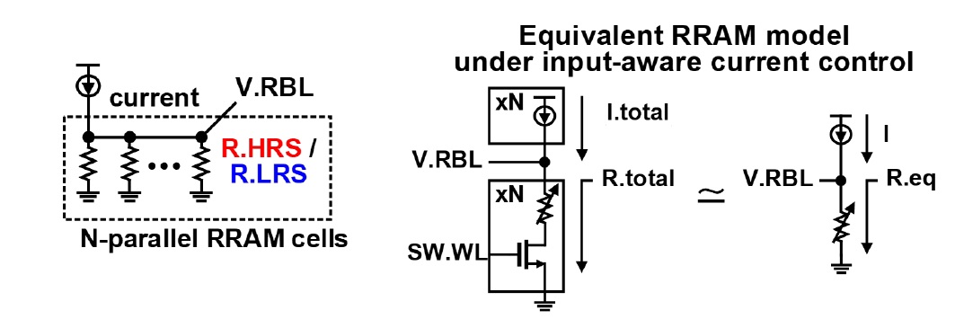
The researchers chose to use an alternative method. Rather than sensing the bitline current (e.g., charging a capacitor for a known duration to develop a readout voltage), the researchers pumped a current into the active bitcells and measured Vbitline directly, as illustrated below.

The effective resistance is the parallel combination of the active LRS and HRS cells. The unique feature is that the current source value is not constant, but is varied with the number of active wordlines – each active wordline also connects to an additional current source input. Feedback from Vbitline to each current source branch is also used, as shown below.

This feedback loop increases the sensitivity of each current source branch to Reffective, thus amplifying the resistance contribution of each (parallel) LRS cell on the bitline, and reducing the contribution of each (parallel) HRS cell. The figure below illustrates how the feedback loop fanout to each current branch improves the linearity of the Vbitline response, with an increasing number of LHS cells accessed (and thus, parallel LRS resistances contributing to Rtotal).

LRS/HRS variation
As alluded to earlier, multiple iterations of write-read are often used, to confirm the written value into the ReRAM cell.

The technique employed here to ensure a tight tolerance on the written HRS and LRS value evaluates the digital value read after the write, and increases/decreases the pulse width of the subsequent (reset/set) write cycle iteration until the (resistance) target is reached, ending the write cycle.
HRS drift
The drift in HRS resistance after many read cycles is illustrated below (measured at high operating conditions to accelerate the mechanism).

To compensate for the drift, each bitcell is periodically read – any HRS cell value which has changed beyond a pre-defined limit will receive a new reset write cycle to restore its HRS value. (The researchers did not discuss whether this “mini-reset” HRS write cycle has an impact on the overall ReRAM endurance.)
Testsite Measurement Data
A micrograph of the ReRAM compute-in-memory testsite (with specs) is shown below.

Summary
ReRAM technology offers a unique opportunity for computing-in-memory architectures, with the array providing the node (data * weight) MAC calculation. The researchers at Georgia Tech and TSMC developed a ReRAM testsite with additional features to address some of the technology issues:
- HRS/LRS variation: multiple write-read cycles with HRS/LRS sensing are used
- low HRS/LRS ratio: a Vbitline voltage-sense approach is used, with a variable bitline current source (with high gain feedback)
- HRS drift: bitcell resistance is read periodically, and a reset write sequence applied if the read HRS value drops below a threshold
I would encourage you to review their ISSCC presentation.
-chipguy
References
[1] Yoon, Jong-Hyeok, et al., “A 40nm 64kb 56.67TOPS/W Read-Disturb-Tolerant Compute-in-Memory/Digital RRAM Macro with Active-Feedback-Based Read and In-Situ Write Verification”, ISSCC 2021, paper 29.1.
Share this post via:


Comments
5 Replies to “Features of Resistive RAM Compute-in-Memory Macros”
You must register or log in to view/post comments.