Background
The emergence of 2.5D heterogeneous die integration using a silicon (or organic) interposer has enabled unique system architectures. The term “More than Moore” has been used to describe the circuit density and cost advantages of leveraging multiple die in the package, the die potentially in different process technologies. Specifically, the integration of High Bandwidth Memory (HBM) stacks has led to innovative product designs, with new memory hierarchy and coherence management approaches.
The efforts to develop “standard” (short-reach and ultra-short-reach) communication interfaces between the heterogeneous die will further promote integration efforts through die re-use.
The EDA tool/platform development required to enable advanced 2.5D integration was relatively minor. There were existing “system-in-package” (SiP) tools for multi-die packages (on organic substrates), such as for the design of separate baseband and radio frequency functions. The density of the redistribution layer interconnects is significantly higher in current 2.5D implementations, yet the additional EDA support for 2.5D package connectivity management, physical implementation, physical design verification, parasitic extraction, and electrical analysis did not involve the introduction of major new features. Such is not the case for the newer 3D package technologies.
An Incremental Approach toward 3D Integration EDA Tool Support
At the recent VLSI Symposium, Vinay Patwardhan, Product Management Group Director in the Digital Design and Implementation team at Cadence, provided insights into the challenges of EDA support for 3D die integration, and the current platform status at Cadence.[1] This article summarizes the highlights of his presentation.
Briefly, 3D packaging technology involves direct, vertical die-to-die attach at bond pad interfaces (i.e., without elevating microbumps). The die orientation may be either face-to-face or face-to-back. Through silicon vias (TSVs) are used to provide connectivity through the die, for face-to-back bonding and to the package substrate. The technology for die bonding is evolving rapidly, currently enabling a connection pitch of ~1um. The TSV density is also potentially very high, with ~5um pitch as the current implementation target. (The supported TSV pitch depends strongly upon the aspect ratio of the via diameter-to-die thickness.)
Vinay divided his presentation into three sub-topics:
- 2D-to-3D algorithm enhancements required for specific tools
- tool-to-tool interdependencies and data interfaces (e.g., for rapid iterative design closure)
- a “comprehensive” 3D design database and tool platform
The figure below illustrates these three areas.
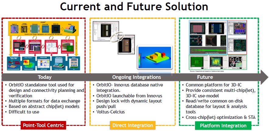
Vinay described that Cadence has taken an incremental approach toward 3D integration enablement, focusing initially on the first two areas, while concurrently developing a common design platform. The goal is to provide an evolutionary path for 3D designers, who are familiar with existing tools.
2D-to-3D algorithm features
Here are a couple of examples of 2D-to-3D tool algorithms features that Vinay described:
- multi-die macro placement
A difficult problem for any placement algorithm is dealing with a (potentially large) number of hard IP macros in the design netlist, in addition to the very large number of standard cells.
As depicted below, a hard IP instance presents significant routing blockages, and typically has few pins. As a result, a wiring-length and (coarse grid) wiring-track density congestion avoidance optimization will tend to place macros toward the perimeter of a floorplan area in a 2D placer.[2]
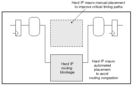
Yet, it is very likely that the hard IP macro is part of timing critical paths, such as the read access time through an on-chip register file or memory array. For timing optimization, the macro should be placed among the related logic cells, despite the few nets involved.
Vinay provided a description of a new 3D placement feature, where hard IP is preferentially promoted to the top die, connected to the related logic through the physical assignment of die-to-die bonds, as illustrated below.

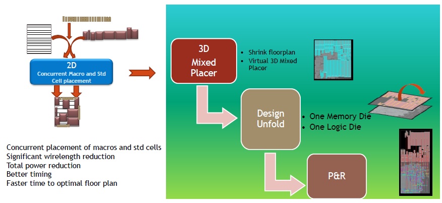
The Innovus implementation tool is “multi-die connectivity aware” as part of its optimization features, with die abstracts representing the different designs.
- 3D system partitioning
An even greater issue with 3D integration design is the initial development of the overall system architecture partitioning between the different die – a task sometimes described as pathfinding. (I had a professor who liked to say, “80% of all electrical design automation challenges are related to partition optimization.”)
Unlike the typical 2.5D design where existing HBM stacks and/or hard IP chiplets are incorporated into the architecture, the 3D system designer is likely working with a blank canvas. The functionality needs to be optimally allocated to individual die to meet PPA and cost objectives.
Vinay described how the Cadence OrbitIO product has been extended to provide the system connectivity model and partitioning analysis features needed for 3D design exploration, as illustrated below.
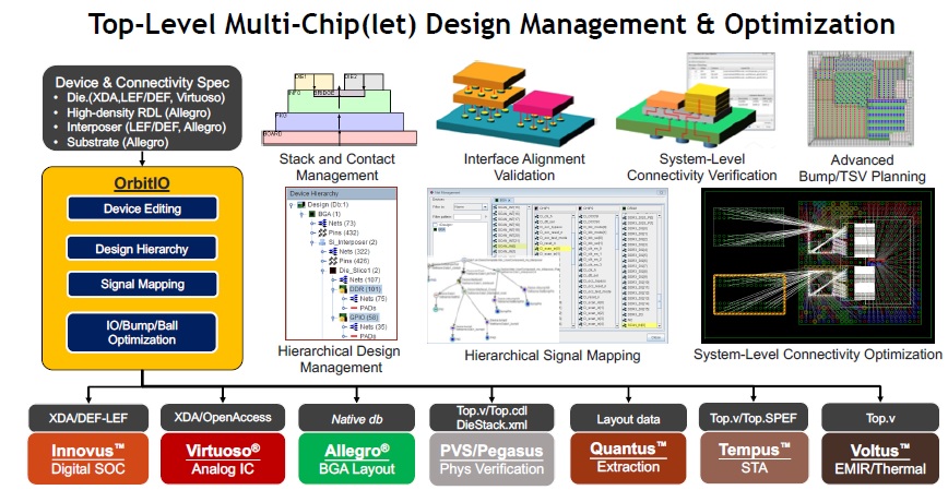
The features added include support for bond and TSV alignment between die and the package substrate, with visualization of the hierarchical system configuration. From the OrbitIO interface, the data exchanges to other tools are also shown in the figure above.
Tool interdependency features for 3D integration
In addition to 2D-to-3D tool algorithm/feature enhancements, Vinay highlighted that Cadence prioritized several key tool interdependencies that necessitated tighter integration, rather than data file export/import.
- iterative design closure for ECOs
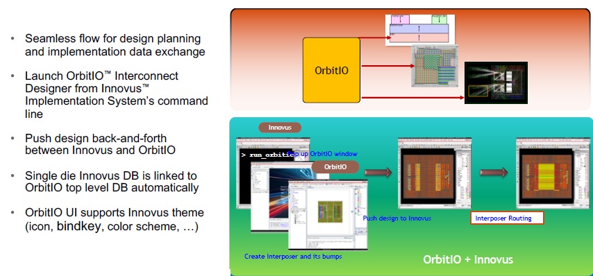
Of specific importance was the integration of the OrbitIO design environment with the Innovus physical implementation tool, such as to support rapid iteration design ECO closure. The figure below shows the additional tool support provided between these two platforms.
- I*R and thermal analysis closure
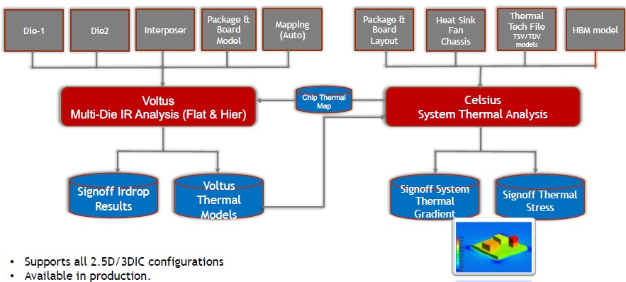
Another tool interdependency focus was extending the 3D capabilities of the power/I*R and thermal analysis data models. Initial 3D power estimates are provided to the 3D thermal analysis engine, which sends thermal map values back to the I*R analysis for design closure, as depicted in the figure below.
3D Platform and ADK Enablement
As shown in the very first figure, the third phase of this EDA flow evolution will be to utilize a full 3D-enabled design database model, to further support inter-die optimizations.
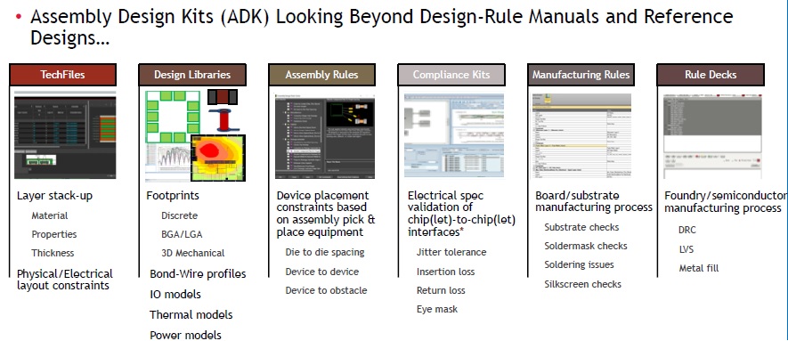
One caveat that Vinay mentioned was the lack of a standard packaging Assembly Design Kit (ADK), analogous to the Process Design Kit (PDK) data that comprehensively represents the fabrication guidelines, electrical models, and design verification rules that define a silicon process. Vinay provided the figure below to illustrate how he envisions an ADK would be integrated into 3D design enablement.
Summary
The evolution of advanced packaging technology to 3D die integration requires significant EDA tool investment. In pursuing an incremental approach, Cadence has added 3D features to tools, and provided specific interdependent tool “tight loop’ iteration support. The remaining verification and analysis flows utilize the data format exchanges shown above. This approach provided full 3D enablement, building upon a mature design platform.
In the future, look for more varied system partitioning techniques, with 2.5D packaging technology integrating 3D configurations – similar to the use of HBM stacks, but with more complex 3D topologies. And, look for increasing momentum behind the definition of an Assembly Design Kit, to accelerate this packaging technology innovation.
-chipguy
References
[1] Vinay Patwardhan, “Entering a new dimension with 3D-IC design – EDA perspective”, VLSI Symposium 2021, Workshop 2.6.
[2] T. Dillinger, VLSI Design Methodology Development, Prentice-Hall, 2019.
Also Read
Neural Nets and CR Testing. Innovation in Verification
Circuit Simulation Challenges to Design the Xilinx Versal ACAP
EDA Design and Amazon Web Services (AWS)
Share this post via:


Comments
There are no comments yet.
You must register or log in to view/post comments.