You are currently viewing SemiWiki as a guest which gives you limited access to the site. To view blog comments and experience other SemiWiki features you must be a registered member. Registration is fast, simple, and absolutely free so please,
join our community today!
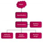
Using chiplets is an emerging trend well-covered at #62DAC and they even had a dedicated Chiplet Pavilion, so I checked out the presentation from Dan Slocombe, Design Engineering Architect in the Compute Solutions Group at Cadence. In a short 20 minutes Dan managed to cover a lot of ground, so this blog will summarize the key points.… Read More
It was back in 1991 that Cadence first announced the Virtuoso product name, and here we are 32 years later and the product is alive and doing quite well. Steven Lewis from Cadence gave me an update on something new that they call Virtuoso Studio, and it’s all about custom IC design for the real world. In those 32 years we’ve… Read More
EDA Flows for 3D Die Integrationby Tom Dillinger on 07-20-2021 at 6:00 amCategories: Cadence, EDA, Events
Background
The emergence of 2.5D heterogeneous die integration using a silicon (or organic) interposer has enabled unique system architectures. The term “More than Moore” has been used to describe the circuit density and cost advantages of leveraging multiple die in the package, the die potentially in different process technologies. … Read More
Semiconductor technology advances have a way of rewriting the rule book. As process geometries shrink, subtle effects graduate to mainstream problems. Performance curves can become inverted. And no matter what else occurs, low power demands are constantly reducing voltage and design margins along with it. Sometimes these… Read More
The recent Design Automation Conference in Las Vegas was an indication of how the electronics industry is evolving. In its formative years, DAC was focused on the fundamental algorithms emerging from academic research and industrial R&D, that enabled the continuation of the Moore’s Law complexity curve. (Indeed, the… Read More
Until recently, ICs at bleeding edge nodes like 7nm technology from foundries like TSMC were mostly targeted for high-performance-computing (HPC) and mobile applications or possibly high radix switches that needed the increased performance of advanced nodes. The momentum of Moore’s law and Moore-than-Moore saw foundries… Read More
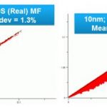
Extraction Features for 7nmby Tom Dillinger on 08-21-2017 at 12:00 pmCategories: Cadence, EDA, FinFET
Frequent Semiwiki readers are familiar with the importance of close collaboration between the foundries and EDA tool developers, to provide the crucial features required by new process nodes. Perhaps the best illustration of the significance of this collaboration is the technical evolution of layout parasitic extraction.… Read More
I’m developing a taste for user-group meetings. In my (fairly) recently assumed role as a member of the media, I’m only allowed into the keynotes, but from what I have seen, vendors work hard to make these fresh and compelling each year through big-bang product updates and industry/academic leaders talking about their work in bleeding-edge… Read More
I talked with Paul Cunningham (VP front-end digital R&D) at CDNLive recently to get a Cadence perspective on digital design trends. He sees needs from traditional semiconductor companies evolving as usual, with disruption here and there from consolidation. But on the system side there is explosion in demand – for wearables,… Read More
It requires lateral thinking in bringing new innovation into conventional solutions to age-old hard problems. While the core logic design has evolved adding multiple functionalities onto a chip, now called SoC, the structural composition of DFT (Design for Testability) has remained more or less same based on XOR-based compression… Read More