IoT Designs Beginning to Shift to 7nm: Promises Upside for Cadence Physically-Aware Design Flow

IoT Designs Beginning to Shift to 7nm: Promises Upside for Cadence Physically-Aware Design Flow
by Mitch Heins on 01-29-2018 at 12:00 pm

Until recently, ICs at bleeding edge nodes like 7nm technology from foundries like TSMC were mostly targeted for high-performance-computing (HPC) and mobile applications or possibly high radix switches that needed the increased performance of advanced nodes. The momentum of Moore’s law and Moore-than-Moore saw foundries… Read More


Extraction Features for 7nm

Extraction Features for 7nm
by Tom Dillinger on 08-21-2017 at 12:00 pm

Frequent Semiwiki readers are familiar with the importance of close collaboration between the foundries and EDA tool developers, to provide the crucial features required by new process nodes. Perhaps the best illustration of the significance of this collaboration is the technical evolution of layout parasitic extraction.… Read More


The CDNLive Keynotes

The CDNLive Keynotes
by Bernard Murphy on 04-25-2017 at 7:00 am

I’m developing a taste for user-group meetings. In my (fairly) recently assumed role as a member of the media, I’m only allowed into the keynotes, but from what I have seen, vendors work hard to make these fresh and compelling each year through big-bang product updates and industry/academic leaders talking about their work in bleeding-edge… Read More


Digital Design Trends – A Cadence Perspective

Digital Design Trends – A Cadence Perspective
by Bernard Murphy on 04-21-2016 at 7:00 am

I talked with Paul Cunningham (VP front-end digital R&D) at CDNLive recently to get a Cadence perspective on digital design trends. He sees needs from traditional semiconductor companies evolving as usual, with disruption here and there from consolidation. But on the system side there is explosion in demand – for wearables,… Read More


Cadence Adds New Dimension to SoC Test Solution

Cadence Adds New Dimension to SoC Test Solution
by Pawan Fangaria on 02-04-2016 at 7:00 am

It requires lateral thinking in bringing new innovation into conventional solutions to age-old hard problems. While the core logic design has evolved adding multiple functionalities onto a chip, now called SoC, the structural composition of DFT (Design for Testability) has remained more or less same based on XOR-based compression… Read More


Globalfoundries 22FDX Technology Shows Advantages in PPA over 28nm Node

Globalfoundries 22FDX Technology Shows Advantages in PPA over 28nm Node
by Tom Simon on 11-20-2015 at 7:00 am

I really enjoy ARM Techcon when it rolls around every year because it has such a wide range of topics and exhibits. You can find maker gadgets, IoT information, small boards for industrial control, software development kits, semiconductor IP vendors as well as the big EDA players and foundries. This year after perusing the exhibit… Read More


Cadence’s New Implementation System Promises Better TAT and PPA

Cadence’s New Implementation System Promises Better TAT and PPA
by Tom Simon on 03-12-2015 at 1:00 am

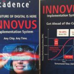
On Tuesday Cadence made a big announcement about their new physical implementation offering, Innovus, during the keynote address at the CDNLive event in Silicon Valley. Cadence CEO Lip-Bu Tan alluded to it during his kick off talk, and next up Anirudh Devgan, Senior Vice President, Digital & Signoff Group, filled in more … Read More


Innovus: Cadence’s Next Generation Implementation System

Innovus: Cadence’s Next Generation Implementation System
by Paul McLellan on 03-11-2015 at 7:00 am

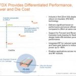
Yesterday was the first day of CDNLive. There were three keynotes. The first was by Lip-Bu Tan, Cadence’s CEO (and the Chairman of Walden International that he will be the first to remind you). The most interesting tidbit was that Cadence now has over 1000 people working on IP and that it represents 11% of their revenue. Then… Read More