Probably one of the most anticipated semiconductor investor calls was held last week and it did not disappoint. It was Lip-Bu Tan’s first full quarter since he took over as CEO. In the resulting discussions on the SemiWiki Forum I am viewed as overly optimistic of Intel’s recent pivot. That is true, I am optimistic, but my observations… Read More

Tag: cadence design systems
Podcast EP213: The Impact of Arteris on Automotive and Beyond with Frank Schirrmeister
Dan is joined by Frank Schirrmeister, vice president of solutions and business development at Arteris. He leads activities in the industry verticals including automotive and technology horizontals like artificial intelligence, machine learning, and safety. Before Arteris, Frank held senior leadership positions at Cadence… Read More
224G Serial Links are Next
The tremendous increase in global data traffic over the past decade shows no sign of abating. Indeed, the applications for all facets of data communications are expanding, from 5G (and soon, 6G) wireless communications to metropolitan area networks serving autonomous vehicles to broader deployment of machine learning algorithms. … Read More
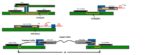
EDA Flows for 3D Die Integration
Background
The emergence of 2.5D heterogeneous die integration using a silicon (or organic) interposer has enabled unique system architectures. The term “More than Moore” has been used to describe the circuit density and cost advantages of leveraging multiple die in the package, the die potentially in different process technologies. … Read More
Podcast EP16: Hyperscale Computing & Changes in the Datacenter
Dan is joined by Frank Schirrmeister, senior group director of solutions marketing at Cadence Design Systems, Frank has extensive experience in complex system design from his work at companies such as Cadence, Synopsys, Imperas and ChipVision. He has also advised Vayavya Labs and CriticalBlue.
Dan and Frank discuss the many… Read More
Webinar: Design Methodologies for Next-Generation Heterogeneously Integrated 2.5/3D-IC Designs
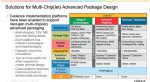
I had the opportunity to preview the upcoming SemiWiki webinar titled: Design Methodologies for Next-Generation Heterogeneously Integrated 2.5/3D-IC Designs. John Park’s message, describing this powerful Cadence solution, really impressed me. That’s why I want to encourage you to register for it and join this SemiWiki … Read More
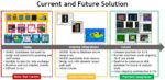
Ultra-Short Reach PHY IP Optimized for Advanced Packaging Technology
Frequent Semiwiki readers are no doubt familiar with the rapid advances in 2.5D heterogeneous multi-die packaging technology. A relatively well-established product sector utilizing this technology is the 2.5D integration of logic die with a high-bandwidth memory (HBM) DRAM die stack on a silicon interposer; the interposer… Read More
IP Provider Vidatronic Embraces the ClioSoft Design Management Platform

Having worked at several semiconductor intellectual property (SIP) companies, I know how important it is to have a strong design data management platform for tracking the development and distribution of SIP products. Everyone doing semiconductor design should care about design data management. But for an IP company, it is … Read More
1-on-1 with Anirudh Devgan, President, Cadence

At the Design Automation Conference, no one is busier than an EDA company executive — conference panels, product launch briefings, customer meetings, and corporate dinners all place considerable demands on their time. I was fortunate enough to be able to meet with Anirudh Devgan, President of Cadence, at the recent DAC55 in San… Read More
IoT Designs Beginning to Shift to 7nm: Promises Upside for Cadence Physically-Aware Design Flow

Until recently, ICs at bleeding edge nodes like 7nm technology from foundries like TSMC were mostly targeted for high-performance-computing (HPC) and mobile applications or possibly high radix switches that needed the increased performance of advanced nodes. The momentum of Moore’s law and Moore-than-Moore saw foundries… Read More