You are currently viewing SemiWiki as a guest which gives you limited access to the site. To view blog comments and experience other SemiWiki features you must be a registered member. Registration is fast, simple, and absolutely free so please,
join our community today!
The ability to extend photolithography utilizing 193i light sources to current process nodes is truly the key technical achievement that has enabled Moore’s Law to continue. The interplay between the exposure equipment, the materials – especially, resists and related coatings – and the fundamental principles… Read More
Introduction to FinFET Technology Part IIIby Tom Dillinger on 11-21-2012 at 5:30 pmCategories: FinFET, General
The preceding two Semiwiki articles in this thread provided an overview to the FinFET structure and fabrication. The next three articles will discuss some of the unique modeling requirements and design constraints that FinFET’s introduce, compared to planar FET technology.
Due to the complexity of FinFET modeling – … Read More
Thanks to SemiWiki readers for the feedback and comments on the previous “Introduction to FinFET Technology” posts – very much appreciated! The next installment on FinFET modeling will be uploaded soon.
In the interim, Dan forwarded the following link to me “ Intel’s FinFETs too complicated and difficult, says … Read More
The previous post in this series provided an overview of FinFET devices. This article will briefly cover FinFET fabrication.
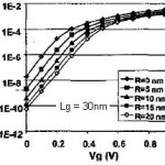
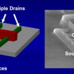
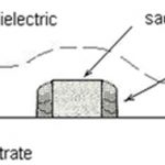
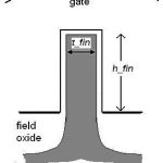
The major process steps in fabricating silicon fins are shown in Figures 1 through 3. The step that defines the fin thickness uses Sidewall Image Transfer (SIT). Low-pressure chemical vapor (isotropic)… Read More
This is the first of a multi-part series, to introduce FinFET technology to SemiWiki readers. These articles will highlight the technology’s key characteristics, and describe some of the advantages, disadvantages, and challenges associated with this transition. Topics in this series will include FinFET fabrication,… Read More


TSMC CoWoS versus Intel EMIB Semiconductor Packaging