The preceding two Semiwiki articles in this thread provided an overview to the FinFET structure and fabrication. The next three articles will discuss some of the unique modeling requirements and design constraints that FinFET’s introduce, compared to planar FET technology.
Due to the complexity of FinFET modeling – and Dan’s guidelines to “keep it short, or they won’t read it” 🙂 – this discussion will be divided into three SemiWiki articles. This post will cover modeling the device itself. A subsequent post will discuss modeling the device parasitics. The final post in this thread will discuss some of the CAD flow impacts associated with introduction of FinFET’s.
Spice models
Recently, the Compact Model Council approved the standardization of the BSIM-CMG FinFET model, based upon the outstanding work from the Spice team at UC-Berkeley. I would encourage SemiWiki readers interested in FinFET’s to read the documentation on the BSIM-CMG model:
http://www-device.eecs.berkeley.edu/bsim/?page=BSIMCMG
(Links: “Latest Release”, then “Technical Manual”)
In particular, note that parallel fins are represented in the BSIM-CMG model using a parameter “NFINS = n” – that will have implications in modeling device parasitics and in CAD flows.
Device behavior
This brief discussion of device behavior will be divided into three sections: (1) the subthreshold “off” leakage current (Ioff); (2) the active current; and, (3) the factors that will introduce variation into the device behavior.
[LIST=1]
One of the key issues in scaling planar FET technology has been the process engineering required to minimize subthreshold current. With power dissipation (and standby battery life) such a critical factor in product design, the focus on minimizing Ioff is very high.
The subthreshold leakage current is strongly dependent upon the threshold voltage (Vt), gate length (Lgate), temperature, and process fabrication. (Recall that the transistor width of an individual fin is fixed.) There are a number of methods for measuring “Vt” – the most common definition is the input Vgs voltage when a specific device current Ids is present (small Vds voltage difference). Below this Vgs threshold, the device current falls exponentially with input voltage. The process dependence of this exponential relation for Ioff is typically represented as the subthreshold slope parameter, S, which is in units of mV/decade (at a given temperature). A small S value is preferable – a smaller change in gate input voltage will reduce the leakage current by a factor of 10.
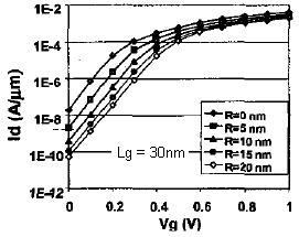
The strong electrostatic control of the gate terminal over the FinFET channel results in a smaller S value than comparable planar FET’s, for fins of an appropriate thickness and impurity concentration. The gate-to-channel electric field is concentrated at the fin corners. As a result, as the gate-to-source input voltage increases toward the device threshold, there will be a higher concentration of subthreshold leakage current at the corners of the fin, aka the “corner effect”, as depicted in Figure 1.

Figure 1. Subthreshold leakage current increases for fins with a smaller radius of curvature at the corners. From Doyle, et al, “Tri-Gate Fully Depleted CMOS Transistors”, VLSI Technology Symposium, 2003, p. 133-4.
Recent SemiWiki articles have highlighted that the initial FinFET’s devices in production have a more tapered and rounded profile – in addition to being easier to fabricate, the (sub-threshold) current crowding effect at the corners will be reduced.
[LIST=1]
The BSIM-CMG model has numerous parameters, to accurately model the active FinFET device current. There’s not enough space to go into detail on the characteristics of this model – yet, there are two things to highlight, one included and one noticeably absent in this (first generation) model.
The FinFET thickness is a key manufacturing parameter. (A previous SemiWiki article in the series talked about a “sidewall image transfer” process step, which defines the fin thickness – this will be the same for all devices.)
If the FinFET is too thick, the electrostatic influence of the gate on the sides and top of the fin will be weaker, and the fin body will behave more like a (planar device) bulk substrate, losing the benefits of the FinFET topology.
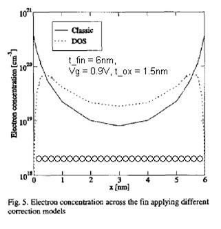
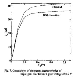
If the FinFET is very thin, a special phenomenon results – the “density of available electron (or hole) states” is reduced. Briefly, free electrons/holes conduct current in the transistor channel, by having sufficient energy to reside at the conduction/valence energy band edges of the semiconductor material. The electron/hole energy and band levels in the semiconducting silicon are strong functions of the applied voltages and temperature, which are the basis for the FET model. Normally, there is no shortage of available “free states” for energetic electrons/holes at the band edges. However, for very thin fins, there is a quantum phenomenon which will reduce the density of available states at the band edge. As a result, electrons/holes would need more energy to occupy available states higher than the band edge, and be free to conduct device current. The BSIM-CMG model includes corrections for the “quantum density of states” for thin fins. Figure 2 illustrates the reduced free electron concentration and Figure 3 depicts the corresponding device current reduction due to the quantum density of states.

Figure 2. Free electron concentration reduction in fin cross-section, for the quantum density of states (t_fin = 6nm, approx. 25 atomic layers). From Entner, et al, “A Comparison of Quantum Correction Models for Three-Dimensional Simuatltion of FinFET Structures”, 27th Int’l. Seminar on Electronics Technology, 2004, p. 114-7.

Figure 3. Device current correction, accounting for the quantum density of free electron states. Same reference as Figure 2.
Conversely, there is one BSIM-CMG feature that is not yet included. Designers working with recent planar FET technologies and BSIM-4 models are very cognizant of “layout dependent effects” (LDE), and their influence upon the device current. New terms such as the “well proximity effect” (due to well implant impurity dosage scattering) and several “spacing effects” (due to the localized influence of additional “stress” materials and shallow-trench isolation on the channel carrier mobility) have been added to models.
CAD flows for planar technologies offer (early) cell layout automation features to estimate the LDE measures. This automation is applied when designers are still conducting initial feasibility simulations, well before detailed layouts are available for parasitic extraction.
FinFET technology is still in its relative infancy. There is little (published) work on LDE’s with FinFET’s, and as a result, there are no parameters in the BSIM-CMG model. Foundries will need to work very closely with design teams and Spice simulation vendors to define and enable LDE correction factors.
[LIST=1]
There’s not enough space in this brief post to delve into sources of FinFET variation.
There are numerous fabrication steps that will affect the device behavior. As mentioned above, the actual fin geometry defines the main device behavior, and each will have its (local and global) variation tolerances – e.g., fin thickness, height, sidewall profile, sidewall roughness, gate roughness.
There are alternatives for offering multiple device Vt thresholds, each with their own sources of variation – i.e., different metal gate compositions that provide workfunction potential differences and/or impurity implants into the FinFET body.
Suffice it to say that designers will need to understand the derivation of “process corner models” from their foundry. Circuit designs that need a more sophisticated statistical approach – e.g., “weak bit” SRAM or flip-flop stability analysis – will need to work with their foundry on the appropriate parameter distributions and sampling techniques.
A subsequent article will focus on issues related to modeling FinFET parasitics.
As always, thanks for SemiWiki readers for their comments and feedback!
Also read:
Introduction to FinFet Technology Part I
Introduction to FinFet Technology Part II


Is Intel About to Take Flight?