You are currently viewing SemiWiki as a guest which gives you limited access to the site. To view blog comments and experience other SemiWiki features you must be a registered member. Registration is fast, simple, and absolutely free so please,
join our community today!
The way we are seeing technology progression these days is unprecedented. It’s just about six months ago, I had written about the intense collaboration between ANSYSand TSMCon the 16nm FinFET based design flow and TSMC certifying ANSYS tools for TSMC 16nm FF+ technology and also conferring ANSYS with “Partner of the Year” award.… Read More
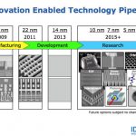
In the modern semiconductor ecosystem we are seeing rapid advancement in technology breaking past once perceived limits; 28nm, 20nm, 16-14nm, 10nm and we are foreseeing 7nm now. Double and multi-patterning are already being seen along with complex FinFET structures in transistors to gain the ultimate advantages in PPA from… Read More
No doubt that FDSOI generate high interest these days and I found a very interesting contribution from Zvi Or-Bach, President and CEO of MonolithIC 3D, Inc. Zvi has accepted to share his wrap-up from IEDM, in a blog for Semiwiki readers. If you remember the long discussion we had in Semiwiki about cost comparison, some comments were… Read More
The biggest surprise embedded in the Intel 22nm SoC disclosure is that they still do NOT use Double Patterning which is a big fat hairy deal if you are serious about the SoC foundry business. The other NOT so surprising thing I noticed in reviewing the blogosphere response is that the industry term FinFET was dominant while the Intel… Read More
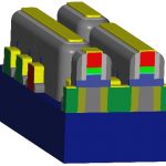
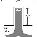
Introduction to FinFET Technology Part IIIby Tom Dillinger on 11-21-2012 at 5:30 pmCategories: FinFET, General
The preceding two Semiwiki articles in this thread provided an overview to the FinFET structure and fabrication. The next three articles will discuss some of the unique modeling requirements and design constraints that FinFET’s introduce, compared to planar FET technology.
Due to the complexity of FinFET modeling – … Read More
At advanced process nodes, variation and its effects on the design become a huge challenge. Join Cadence® Virtuoso® experts for a series of technical webinars on variation-aware design. Learn how to use advanced technologies and tools to analyze and understand the affects of variation. We’ll introduce you to the latest Virtuoso… Read More
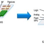
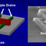
Intel is the number one semiconductor company in the world and has taken the lead in bringing FinFET (aka Tri-Gate) silicon to market at the 22nm node starting in May 2011, so now we see the pure play foundries playing catch-up and start talking about their own FinFET roadmaps. IC designers and layout engineers want to know how their… Read More
Thanks to SemiWiki readers for the feedback and comments on the previous “Introduction to FinFET Technology” posts – very much appreciated! The next installment on FinFET modeling will be uploaded soon.
In the interim, Dan forwarded the following link to me “ Intel’s FinFETs too complicated and difficult, says … Read More
Ever since the “Intel Reinvents Transistors Using New 3-D Structure” PR campaign I have been at odds with them. As technologists, I have nothing but respect for Intel. The Intel PR department, however, quite frankly, is evil. Correct me if I’m wrong here but Intel did not “reinvent” the transistor. Nor did they come up with the name… Read More
This is the first of a multi-part series, to introduce FinFET technology to SemiWiki readers. These articles will highlight the technology’s key characteristics, and describe some of the advantages, disadvantages, and challenges associated with this transition. Topics in this series will include FinFET fabrication,… Read More