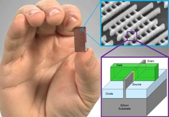
 Ever since the “Intel Reinvents Transistors Using New 3-D Structure” PR campaign I have been at odds with them. As technologists, I have nothing but respect for Intel. The Intel PR department, however, quite frankly, is evil. Correct me if I’m wrong here but Intel did not “reinvent” the transistor. Nor did they come up with the name Tri-Gate. If not for prior art, Intel would certainly have trademarked it, my opinion.
As I previously wrote, other than the unique profile chosen by Intel for their Tri-Gate implementation, there really is no key technical distinction between Tri-Gate and the industry standard term FinFET. According to Dan Hutcheson, CEO of VLSI Research, who follows Intel rather closely:
The reason why Intel calls its FinFET a Tri-Gate is that it is a subspecies of the technology. The original FinFET was a bigate. When Intel first developed theirs (way back in the last decade) out of respect for Chenming they named it a Tri-Gate, so as not to draw from UCB’s work. Out of respect? What does that say about the rest of the industry drawing from Chenming’s work that is using the FinFET moniker? Plus, Dan says, the real importance of the Tri-Gate is not so much the third gate, but the fact that it is so much easier to manufacture than a bi-gate. That was the real contribution of Intel. 
According to my sources this is not entirely true. The original paper(s) from Chenming’s group at UC-B did propose a “dual gate” (possibly even independent) structure. In the original proposal, the top surface of the FinFET would receive a thicker dielectric than the sidewalls, and not contribute to the device current. If the fin was covered by a single, continuous gate material, that would be a “dual gate”. If the gate material was etched and the sidewalls were covered by separate gates, that would be an “independent dual gate”. (Offering two independent input signals to a FinFET device provides some unique power/performance tradeoff optimizations not available with a single input signal to the transistor.)
However, lots of researchers pursuing FinFET fabrication realized that the “dual” gate (especially the dual-independent option) would be very difficult to fabricate with high yield in production. As a result, technical papers began to emerge with the triple-gate option, where the (thin) gate dielectric was also present on top of the fin, in addition to the sidewalls. The third gate surface on top of the fin is not as effective as the gate on the two sidewalls, as your note indicates.
Here’s an example of some of the triple-gate research:
Burenkov and Lorenz, “Corner effect in double and triple gate FinFET’s”, 33rd Conference on European Solid-State Device Research, 2003, p.135-138.
So, Intel was among many to pursue triple gate FinFET fabrication. And, they were certainly not the only research team to use the term “tri-gate” 10+ years ago:
Breed and Roenker, “Dual-gate and Tri-gate FinFET’s: Simulation and Design”, International Semiconductor Device Research Symposium, 2003, p. 150-151.
So, the use of the term is not really in deference to Chenming or UC-B — it’s a “de facto” standard term that the industry has used for the FinFET fabrication option that Intel has chosen.
Share this post via:


Comments
10 Replies to “Industry Standard FinFET versus Intel Tri-Gate!”
You must register or log in to view/post comments.