You are currently viewing SemiWiki as a guest which gives you limited access to the site. To view blog comments and experience other SemiWiki features you must be a registered member. Registration is fast, simple, and absolutely free so please,
join our community today!
While there is a lot of excitement around the semiconductor shortage narrative and the fabs all being full, both 200mm and 300mm, there is one big plot hole and that is the FinFET era.
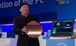
Intel ushered in the FinFET era only to lose FinFET dominance to the foundries shortly thereafter. In 2009 Intel brought out a 22nm FinFET wafer at the… Read More
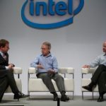
Bill Holt’s “Advancing Moore’s Law” presentation at the recent Intel Analyst day was swallowed hook, line, and sinker by the mainstream media fish so let me play devil’s advocate here and point out some problems with his spin on the competitive landscape.
Coincidentally, one of my Intel friends insists that Intel is number one … Read More
There was an article on Motley Fool recently detailing Intel’s 14nm FinFETs and comparing them to TSMC. Unfortunately the author has zero semiconductor education or experience even though he writes with authority on all things semiconductor. He also has no shame in using outdated papers from conferences he did not even… Read More
A Brief History of FPGAsby Daniel Nenni on 08-26-2012 at 7:30 pmCategories: FPGA
From the transistor to the integrated circuit to the ASIC, next comes programmable logic devices on the road to the mainstream fabless semiconductor industry. PLDS started in the early 1970’s from the likes of Motorola, Texas Instruments, and IBM but it wasn’t until Xilinx brought us the field programmable gate array (FPGA)… Read More
Ever since the “Intel Reinvents Transistors Using New 3-D Structure” PR campaign I have been at odds with them. As technologists, I have nothing but respect for Intel. The Intel PR department, however, quite frankly, is evil. Correct me if I’m wrong here but Intel did not “reinvent” the transistor. Nor did they come up with the name… Read More
Clever title but it’s not mine. Piper Jaffray Analysts Auguste Richard and Jennifer Baxter released a report last week which echoed the concerns of others, including myself. The concerns reported are with the 22nm process and not the chipsets themselves. To me this is all part of ramping a leading edge process but the concerns are… Read More
Since the last Intel logo parody went over so well here is another one! Not so much a parody in light of the recent PR from Intel that the fabless semiconductor business model is doomed. As one of the doomed little people inside the fabless ecosystem I take exception to this but I digress….
The word around Silicon Valley is that Intel … Read More
This just in from Tech Trader Daily, quoting Piper Jaffraychip analyst Gus Richard:
The whole issue for Qualcomm, based on Richard’s conversations with industry types, is that the company has started making its “MSM8960″ chip with Taiwan Semiconductor Manufacturing (TSM) only two to three quarters after TSM introduced… Read More
There is an interesting discussion in the SemiWiki forum in response to the EETimes article: Intel exec says fabless model ‘collapsing’. Definitely an interesting debate, one worth our time since the advertising click hungry industry pundits will certainly jump all over it. Clearly I’m biased since I helped build… Read More
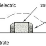
The previous post in this series provided an overview of FinFET devices. This article will briefly cover FinFET fabrication.
The major process steps in fabricating silicon fins are shown in Figures 1 through 3. The step that defines the fin thickness uses Sidewall Image Transfer (SIT). Low-pressure chemical vapor (isotropic)… Read More