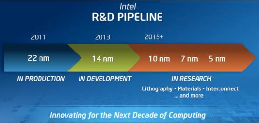
 Since the last Intel logo parody went over so well here is another one! Not so much a parody in light of the recent PR from Intel that the fabless semiconductor business model is doomed. As one of the doomed little people inside the fabless ecosystem I take exception to this but I digress….
The word around Silicon Valley is that Intel is having manufacturing issues at 22nm. The first indication is product launch delays, but more importantly, the dissection of the 22nm silicon. The conclusions being made are:
[LIST=1]
Bottom line: Moore’s Empirical Observation (Law) is coming back to haunt Intel.
“What would you like your legacy to the world to be? Anything but Moore’s Law!” Gordon Moore May 2008.
If true, this does not surprise me at all. It is common Silicon Valley knowledge that Intel uses ultra-restrictive process methodologies. That is why they get different results than the foundries using the same semiconductor manufacturing equipment. Ultra-restrictive methodologies work fine when you are manufacturing one product (microprocessors), but the foundry business and mobile SoCs do not have that luxury.

The troubling part of this whole thing is that Intel’s problems with Tri-Gates have a much broader implication as there really is no major distinction between Intel’s term “Tri-Gate”, and the industry standard “FinFET”. The thin oxide on the top of the fin enables a (small) increment to the device width, when added to the height of the fin sidewalls — a third, or “Tri-” gate, if you will.
The term “FinFET” refers to either the three thin-oxide surfaces or a different fabrication option that results in a thick oxide on the top of the fin, and thus a “dual” gate device consisting of the two fin sidewalls only.
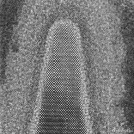
 However, in practice, there are some unique characteristics of Intel’s implementation that are coming to light. There are some interesting Transmission Electron Microscope (TEM) photographs of Intel’s Ivy Bridge devices that have been posted by the engineering analysis team at Chipworks.
The design community (outside Intel) is a little surprised at the extent to which the fin sidewall profile on Intel’s devices is very sloped, almost resulting in a triangular rather than rectangular cross-section. No doubt, that simplifies fabrication, but most certainly complicates the extraction and device modeling requirements.
Other than that “unique” profile chosen by Intel for their “Tri-Gate” implementation, there really is no key distinction between “Tri-Gate” and the industry standard term “FinFET”.
Intel is absolutely on the bleeding edge of FinFET manufacturing so I hope we are all sympathetic to their plight. Lets minimize the drama, learn from it, and move this technology forward as quickly as possible.
Share this post via:


Comments
11 Replies to “Intel Tri-Gate is in Trouble?!?!?!”
You must register or log in to view/post comments.