
The annual International Electron Devices Meeting (IEDM) took place last month. One of the presentations on the short course was by Matthew Metz of Intel titled New Materials Systems for Moore’s Law Continuation. In essence this was a look at some of the possibilities for what comes after silicon runs out of steam.

Matthew started with a look at how the transistor has changed the world and, in particular, the materials innovations that have driven Intel’s own process roadmap over the decades. Back at 90nm we had strained silicon, followed by HiK metal gate. Intel was the first to market with FinFET (although back then it called it TriGate). At Intel 4, EUV lithography was first introduced.

As you probably know, Intel is doing technology development of 5 processes in 4 years, which is obviously aggressive, but apparently is all still on track. Intel 20A will be the first process with gate-all-around (GAA) which Intel calls ribbonFET. Intel also has an aggressive advanced packaging roadmap, but I’m going to skip that since the focus of the talk was what are we going to put on the wafers in the future, not how we will put them together.

Intel is not alone in going for gate-all-around. Over the last couple of years at conferences like IEDM, all the major manufacturers and research organizations have published some version of nanosheet gate-all-around results. See the cross sections above.
The next big innovation planned is complementary FET or CFET, with n-transistors over p-transistors. In fact this was almost the theme of this year’s IEDM with many people announcing various innovations in the manufacture of CFET to get a 1.5X to 2X area scaling.

Another innovation that Intel is pursuing (along with everyone else) is backside power delivery network (backside PDN) along with what Intel calls PowerVia. These technologies allow for signals and power to be separated and no longer interfere with each other as has historically been the case, when all the interconnect was on the front side (well, the only side until recently).
The biggest challenge is the power wall. It is very difficult to get more than 100W per square centimeter of cooling. There are various possibilities as to how to improve things:
- Conventional MOSFET enhancements
- Strained silicon germanium (SiGe) nanoribbons
- Ge or InGaAs nanoribbons
- Tunnel FETs
- Dirac FETs (graphene and 2D)
- Negative capacitance NCFET
- In-memory compute with FerroTunnel Junction or FerroFET

There are a lot of attractions to doing 2D materials instead of sticking with 3D. But there are major challenges with finding good materials. I’m sure you’ve heard of carbon nanotubes (CNT) but despite the attraction there has been no real advance in the challenge of manufacturing these reliably for ten years. Graphene is 2D but has no bandgap making building switches a challenge. Phosphorene is volatile at high temperature making manufacturing a complete transistor impossible.

The most attractive solution seems to be development of transition metal dichalcogenides or TMD. I confess that this was the first time I’d heard of these, at least under this name. It is one of the more promising approaches using 2D materials. TMD are a single monolayer giving good gate-control so lower power. They have better mobility than silicon, so good performance. Also, a large bandgap so limited source-drain tunneling.
Matthew went into quite a lot of detail about the challenges and promises of manufacturing TMD 2-layer transistors, in particular growing 2D single layer transistors, and how to contact them. For contants to the n-transistor the most attractive materials seem to be antimony (Sb) and Bismuth (Bi). For the p-transistor, ruthenium (Ru).

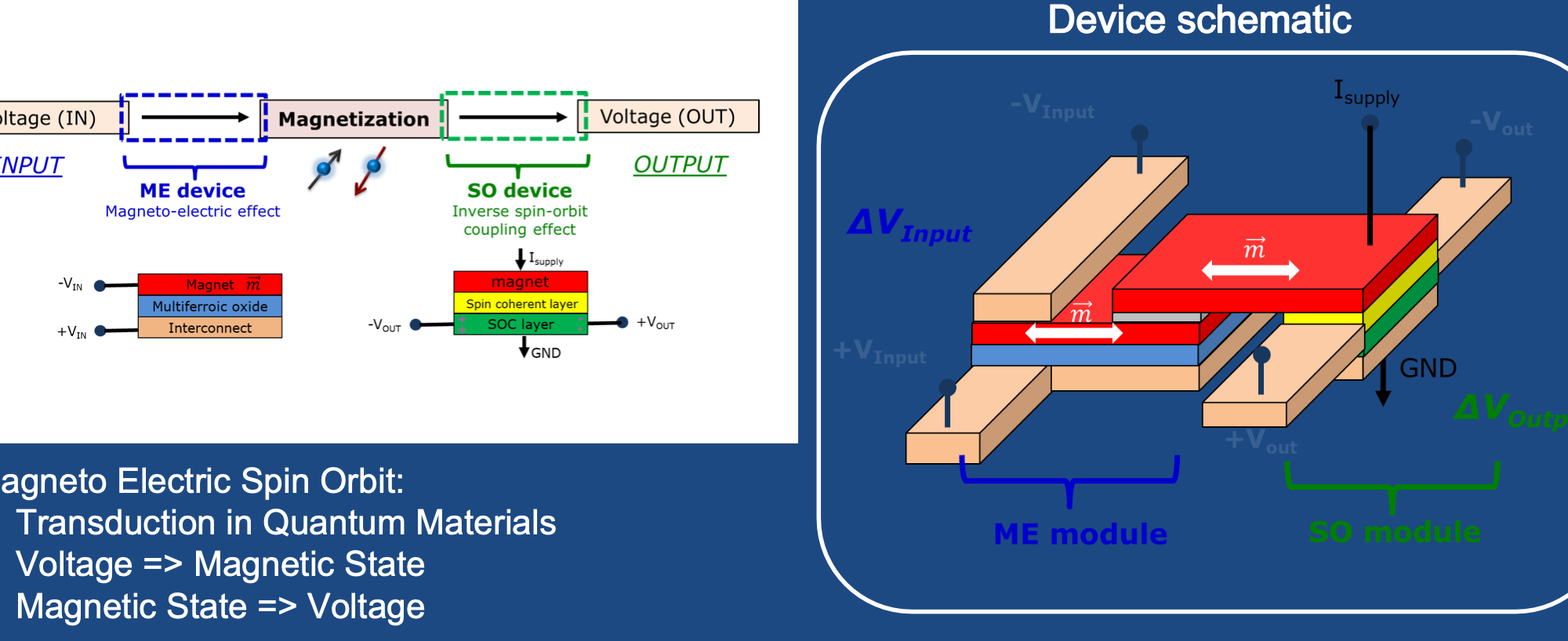
The last section was a look at scaling down power requirements and advanced switching, in particular the magneto-electric spin-orbital (MESO) devices. Switching can be done at around 0.1V with corresponding power reduction.
Matthew’s conclusion is that work going on at Intel with TMD shows promise for continued CMOS scaling, and MESO devices have a lot of promise for drastic power reduction. But this is comparatively early research and there is a lot of work still to be done to make either of these technologies a practical reality.
Also Read:
2024 Big Race is TSMC N2 and Intel 18A
IEDM Buzz – Intel Previews New Vertical Transistor Scaling Innovation
Intel Ushers a New Era of Advanced Packaging with Glass Substrates
Share this post via:


Comments
There are no comments yet.
You must register or log in to view/post comments.