


Clever title but it’s not mine. Piper Jaffray Analysts Auguste Richard and Jennifer Baxter released a report last week which echoed the concerns of others, including myself. The concerns reported are with the 22nm process and not the chipsets themselves. To me this is all part of ramping a leading edge process but the concerns are real and should be discussed.
You can start with SemiWiki blogs:
Piper Jaffray Analyst Spanks Intel
Intel is Selling Itself Short on TriGate
Intel TriGate is in Trouble?!?!?!
And move onto the latest Piper Jaffray Report:
“Based on competitive engineering analysis, simulations, benchmarks and conversations with experts, we believe Intel will have difficulty scaling its FinFET process to 14nm without major modifications or developing an SoC process needed for smartphones. We believe the primary issue is that a moderately doped channel offers better immunity from performance variation caused by the FinFET profile. However, given the small volume of the FinFET transistor channels, there are only a handful of dopant atoms making process control difficult and creating variation and performance issues. In addition, these effects force chips to operate with a single threshold voltage and multiple threshold voltages are needed in SoC devices for I/O and other non processor functions.”
I am also spending time with the FinFET experts and agree with the above statement 100%. Intel may have gotten ahead of themselves on 14nm PR. SemiWiki has a designer who is writing a series on FinFETs HERE. I work with Berkeley Design Automation, they are on the forefront of FinFET modeling and Solido Design Automation on process variation analysis. Bottom line, there are more FinFET questions than answers today. This is bleeding edge technology and there is plenty more blood to come.
“The power consumption is coming in higher than expected. Ivy Bridge is more sensitive to voltage than Sandy Bridge and Ivy Bridge runs hotter than its predecessor when overclocked. This allows the older generation to match the performance under these conditions. This suggests Ivy Bridge is primarily a shrink of Sandy Bridge implying Intel has a process limitation rather than a design issue. Moreover, Intel always launches high margin server and notebooks first on a new process. Intel downplayed the fact that its server line was out first, obscuring the fact it was delayed six months. We think the delay of Romley was not a chipset problem, but a process problem. Moreover, some companies tied to the Romley ramp have suggested the ramp is slower than expected. Finally, it makes no sense that the company would launch desktop before ultrabooks processors. We think this points to power consumption issues with the 22nm process.”
First, Romley is a 32nm part so I do not see the connection in this context. Second, Power leakage is not just a process problem, it is also a design problem. Just because one design or one company has power problems, that does not necessarily condemn the process. Most often it is a combination of both process and design issues. We saw this at 28nm where most companies yielded but one very loud company did not (NVIDIA). Ivy Bridge is the first design to come off a 22nm FinFET (Tri-Gate) process, there is certainly going to be room for improvement.
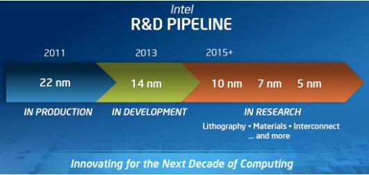
“Intel introduced products based on 90nm, 65nm, 45nm and 32nm in Q4 of 2003, 2005, 2007, and 2009 respectively. The 22nm product was introduced in Q2:12 – six months late. Based on conversations with contacts, the 22nm SoC is now expected to be in production in mid-2013, a year or more late. Based on conversations, we think it may need to make significant changes to its process at 14nm node. Significant changes may slow its introduction. Our conclusion remains Moore’s Law is slowing and this is likely to have negative margin consequences for Intel. Gross margin would be negatively impacted by low yields of server and ultrabooks. R&D costs would increase as Intel would need to spend more on Moore.”
And form your owns conclusions in the comment section:


Comments
There are no comments yet.
You must register or log in to view/post comments.