Background
Traditionally, the interface between chip designers and system power, packaging, reliability, and mechanical engineering teams was a relatively straightforward exchange of specifications. Chip designers developed preliminary power dissipation estimates, often based on a simplifying power/mm**2 value. Packaging engineers ensured the power distribution network (PDN) to the die was robust – i.e., low impedance across switching transients of interest. And, they developed a thermal resistance model of the die-to-package ambient heat transfer path.
System mechanical engineers developed a model of the product enclosure, and analyzed the overall thermal environment, from conduction through the packages in the system to convection in a fluid environment, such as forced air through the enclosure.
Die attach stress analysis typically consisted of applying thermal transients of maximum range equal to the anticipated number of binary on-off cycles during the product lifetime.
The feedback loop was closed by providing temperature calculations back to the chip designers, to confirm the device junction temperature was within the maximum PVT corner setting. And, once the chip physical implementation was complete, designers applied functional verification switching activity factors to net capacitive loads to confirm the initial power estimates were not exceeded.
Those days of a simple design closure methodology are gone, due to a variety of factors:
- complex intra-die power dissipation profiles
Current SoCs have a multitude of local power domains, block-level sleep/active power states, and dynamic-voltage frequency-scaling (DVFS) operating modes. The thermal die map and thermal gradients across the die are much more complex.
- different thermal dissipation flows from die to package
With the emergence of FinFET and SOI process technologies, the traditional assumption of “all device channel thermal energy dissipates through the bulk substrate” is invalid. Complex thermal resistance models through the metallization stack are required.
- the materials used in BEOL fabrication have changed significantly
Specifically, the introduction of porous low-K dielectrics in the BEOL metallization stack results in a weaker mechanical structure, and a higher risk of fracture and/or delamination between dielectric and metals when subjected to thermally-induced stress.
- 2.5D and 3D advanced packaging technologies have introduced a myriad of new configurations
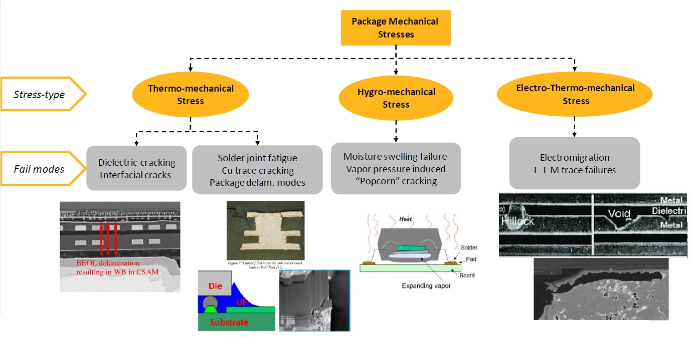
These packages incorporate multiple, heterogeneous die, with topologies that necessitate detailed thermal and mechanical analysis. Specifically, 2.5D packaging uses unique interposer materials, interconnect redistribution layers, and microbumps with through silicon vias (TSVs). This last topology requires special consideration, as it introduces (a large number of) additional thermal/mechanical reliability detractors, as illustrated below.

These package configurations also amplify the significance of multiphysics analysis applied during the initial design exploration phase. The definition of the TSV connections to the interposer (2.5D) or between die (3D) must not only satisfy the physical rules, but also support electrical, thermal, and mechanical constraints. Multiphysics flows are needed (with preliminary models) to develop an initial implementation that enables individual design teams to proceed, confident that tapeout-level analysis closure will not be disruptive.
Thus, there is a need for a new methodology, to provide a more comprehensive analysis of electrical, thermal, and material stress characteristics of an SoC, its package, and the system implementation.
Multiphysics
The foundation of this new methodology relies upon the consistent, coupled analysis of multiple disciplines:
- detailed resistive and dielectric losses from electromagnetic analysis transferred to thermal analysis
- fluid flow interaction with structures
- fluid-solid heat transfer
- materials stress and structural analysis
- reliability analysis
The broad term for this methodology is to apply “multiphysics” simulation across these disciplines – and significantly, unlike the disjoint silos in the engineering methodology described above, these simulations are an integral part of the initial design exploration phase of product development.
I recently had the opportunity to discuss the importance of multiphysics simulation with several members of the Ansys team. This article summarizes our discussion.
2.5D/3D Packaging Simulation
A key consideration in the introduction of a multiphysics methodology is the allocation of modeling and simulation responsibilities among the design team, especially for advanced packaging technologies.
Ankur Gupta, Sr. Director Product Management in the Semiconductor Products group, indicated, “Some customers view 2.5D/3D definition as an extension of chip design tasks, while others view it as an extension of package and system engineering. Flows needs to support multidisciplinary simulations managed from either a chip design-centric or package-centric platform.” Ankur provided the figure below as an illustration of the Multiphysics platform support provided to these design teams.
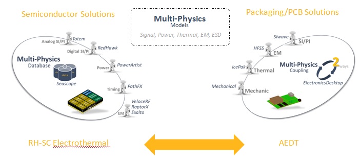
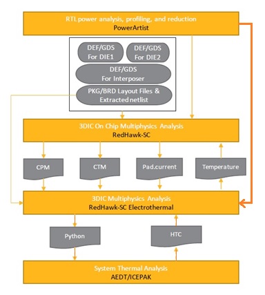
The chip-centric platform on the left incorporates RedHawk-Seascape models, database, and related simulation tools. An example of an early design exploration flow would be to promote preliminary die power models from PowerArtist to the IcePak thermal simulations on the right, as depicted below.
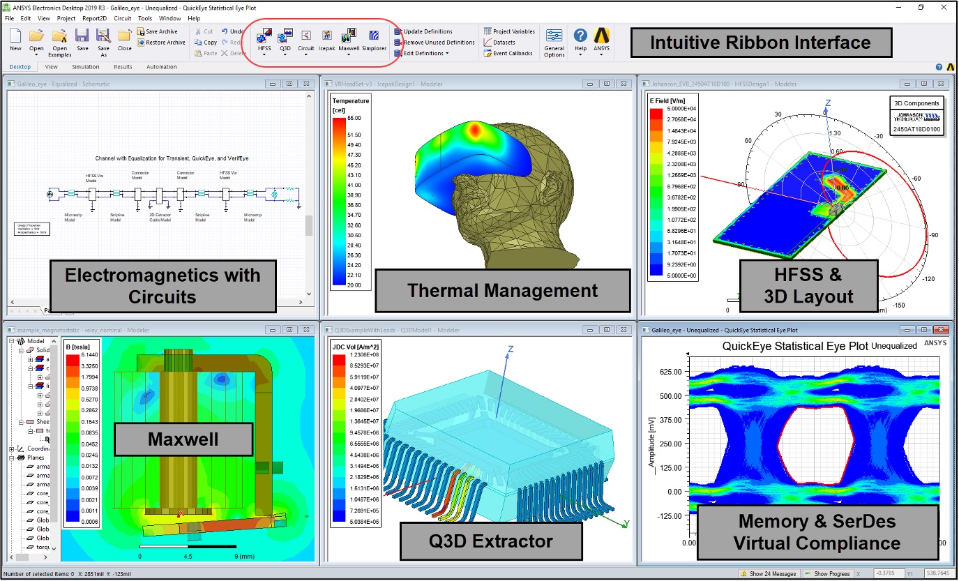
The package/PCB platform on the right in the figure above uses the Ansys Electronic Desktop (AEDT) to manage simulations, as illustrated below.
Multiphysics Simulation Features
Jim Delap, Director of Electronics Product management, elaborated further on some of the fundamental underlying simulation technology:
- encrypted techfile for material properties
Ansys has collaborated with foundries, OSATs, and component providers to provide an encryption/decryption flow for describing proprietary materials characteristics to the multiphysics simulation engines. Key material electrical and mechanical properties, such as the coefficient of thermal expansion (CTE) and elasticity, are able to be securely provided to the simulations by the supplier.
- dynamic meshing
Meshing of the physical structure is key to any solver technology. The tradeoffs to consider when creating the mesh are accuracy versus compute resources/runtime. Dynamic meshing technology adapts the mesh during simulation to represent problems involving boundary motion.
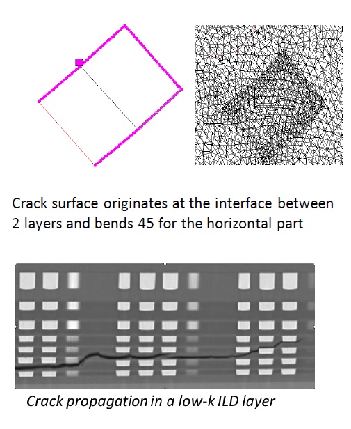
Sooyong Kim, Director Product Specialist in 3DIC Chip Package Systems, offered the example of analyzing cracking in die/package materials due to mechanical stresses. A detailed mesh is needed to accurately evaluate how a (cohesive) fatigue fracture starts, and then a different mesh is used to analyze how that fracture expands. (As a microbump starts to crack, neighboring joints will share more stress and start to crack, as well.)
The figure below illustrates the sources of material stress and the applicable multiphysics analysis techniques.
This next figure illustrates the results of a low-K dielectric crack/delamination simulation.
- sequential and direct coupled analysis
The Ansys Multiphysics methodology incorporates two types of simulations – sequential and direct coupled.
Sequential coupling uses multiple, single-physics models in a unified simulation, thus allowing for dissimilar meshes between models. The interaction between thermal analysis and fluid dynamics is one sequential coupling option. The Ansys Multiphysics analysis platform provides accurate data interpolation between the different meshes.
Direct flows address multiphysics interactions using a single finite element mesh model, with “coupled physics” applied to the mesh elements during simulation. (Note that this approach is ideally suited for non-linear materials properties.) As you might imagine, parallel compute processing capabilities are heavily leveraged.
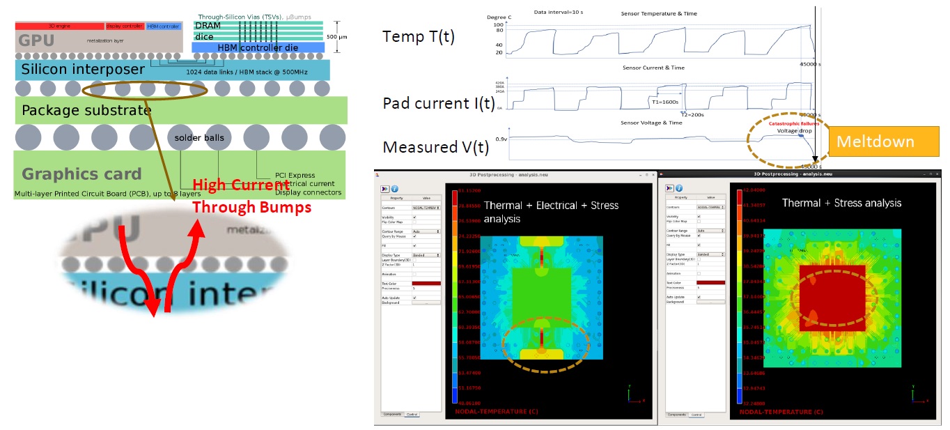
The images on the right in the figure below illustrate the simulation results and thermal map data (including thermal meltdown!) from a direct coupled RedHawk-SC Electrothermal analysis design example.
Summary
System designers are aggressively adopting a coupled multiphysics analysis methodology to replace the traditional silo-like approach. The unique characteristics of the interconnect topologies and materials in advanced multi-die 2.5D and 3D package technologies necessitate a comprehensive approach toward electrical-thermal-structural model simulations. The Ansys Multiphysics platform offers a unified desktop interface toward coupled analysis, with direct-coupled options for fast design exploration and optimization.
For more information on the Ansys semiconductor products, please follow this link. For more information on foundry multiphysics certifications, please refer to these two links: TSMC certification, Samsung certification. Additionally, the Ansys Learning Hub provides a wealth of on-line learning materials – link.
-chipguy
Also Read
There’s No Such Thing as Ground (But Perhaps There’s a Bob) Minimze Your Ports
Bouncing off the Walls – How Real-Time Radar is Accelerating the Development of Autonomous Vehicles
The Electromagnetic Solution Buyer’s Guide
Share this post via:


Comments
There are no comments yet.
You must register or log in to view/post comments.