Introduction
Frequent SemiWiki readers are aware of the growing significance of heterogeneous multi-die packaging technologies, offering a unique opportunity to optimize system-level architectures and implementations. The system performance, power dissipation, and area/volume (PPA/V) characteristics of a multi-die package integration are vastly improved over board-level designs with discrete parts.
The ability to select different technologies for various system functions (as “chiplets”) in the composite 2.5D/3D package adds the dimension of overall product cost to the PPA/V optimization parameters. System development costs are addressed by the potential to leverage chiplet reuse. Production cost assessments address the tradeoff between the additional complexity of 2.5D/3D package design/assembly versus the yield impact of integrating functionality into a single larger die. This tradeoff is influenced strongly if the PPA goals of architectural blocks can be achieved with existing chiplets in older process technologies.
Given these opportunities for system optimization, the diversity of 2.5D implementations (with area >>1X the maximum reticle size) will continue to grow. Similarly, the complexity of 3D stacked die topologies will also increase, with connectivity between the die transitioning from using microbumps to a bumpless, thermo-compression bonded connection between die pads and through-silicon vias (TSVs).
With the emergence of these system-level implementations, there has been a corresponding focus on the requisite EDA flows to support the design planning and configuration management steps. Initially, the 2.5D/3D product teams incorporated a mix of traditional package and SoC implementation tools, passing connectivity and physical models back and forth. The partitioning of the system architecture into chiplets was somewhat ad hoc, often requiring multiple iterations between disparate tools to achieve a routable solution.
The increasing demand for chiplet interface bandwidth and the complexity of the (“short reach”) chiplet interface timing meant that corresponding timing and signal integrity analysis steps need to be an integral part of the initial design process. The higher power dissipation density associated with 3D die configurations also requires thermal analysis to be an early design convergence evaluation.
In short, the growing importance of architectures pursuing 2.5D/3D package implementations necessitates a unified EDA platform, spanning the tasks of system planning to preliminary electrothermal analysis closure.
Cadence Integrity 3D-IC Platform
To address the needs of advanced package design, Cadence recently announced their Integrity 3D-IC platform. I had the opportunity to chat briefly with Vinay Patwardhan, product management group director in the Digital & Signoff Group, about the development and key features of the platform.
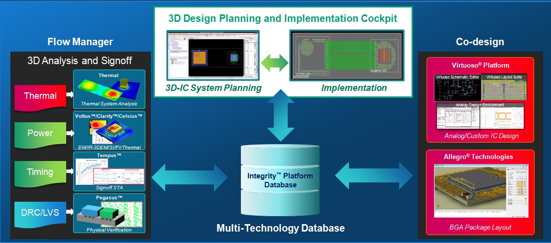
The figure below provides an overview of the platform functionality.

Vinay indicated, “The heart of the Integrity 3D-IC platform is the unified database. The sheer data volume associated with a 3D system design, combined with the tools needed for physical implementation and design rule verification, meant building the Integrity database from IC-based roots. The Cadence Innovus data model served as the foundation, with specific enhancements for Integrity 3D-IC.”
Vinay highlighted the following database features:
- Representation of the partitioned 2.5D/3D model hierarchy
- Support for multiple technology files for the heterogeneous process models for various chiplets
- Integrated version and configuration management to support the system architecture decomposition and optimization
- Maintaining cross-correlation links between physical, timing, and electrical data for pins/nets, pads/bumps, TSVs, and chiplet models
With regards to chiplet models, I asked Vinay about the integration of existing chiplet IP into the system design. He replied, “The Integrity 3D-IC database supports multiple views for a node in the design hierarchy. There are interfaces to import/export standard netlists and model formats, such as Verilog, DEF, LEF, SDCs, boundary model formats like ILM timing abstracts and OpenAccess physical boundary data. Special formats in which package layouts are represented can be read in seamlessly as well.” (More details about the Integrity 3D-IC database are provided in a Cadence white paper. Please refer to the link at the bottom of this article.)
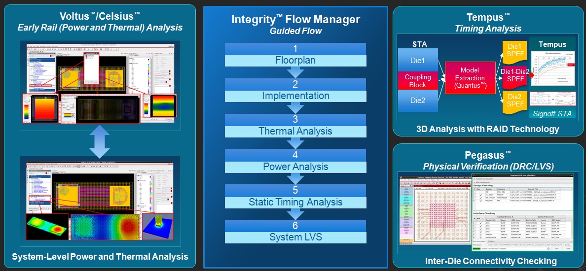
As mentioned above, the confidence in the 3D implementation requires a platform that enables timing, electrical, and thermal analyses to be pursued during the initial system partitioning phase. The figure below depicts the Integrity 3D-IC system-level flow manager, with the corresponding Cadence tool interfaces.

Yet, how do the system architect and packaging engineering teams get started? How can they quickly iterate on early partitioning activities, confident that the bump/pad planning and inter-chiplet connectivity will be realizable before pursuing the analysis flows?
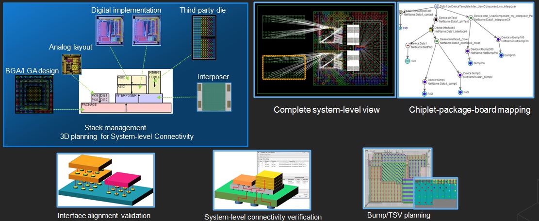
Vinay highlighted a specific feature of the Integrity 3D-IC platform. The system planner GUI is illustrated below, depicting the system architecture in multiple physical and connectivity views.

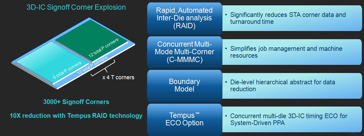
Vinay delved into a key innovation in Cadence’s Tempus Static Timing Analysis (STA) that can be called through the Integrity 3D-IC platform. Specifically, with many discrete heterogeneous die incorporated into the package, the potential number of timing analysis “corners” multiplies quickly, potentially in the thousands. The figure below highlights the issue along with the technology developed to address this specific challenge.

Vinay said, “The Tempus STA tool supports boundary models in conjunction with concurrent, multi-mode, multi-corner (C-MMMC) analysis for data reduction and to simplify job management. On top of that, we have added a special feature called rapid, automated inter-die (RAID) analysis, which is a ‘smart pruning’ feature to reduce the number of analysis corners designers need to consider when performing 3D timing analysis in Integrity 3D-IC.”
I asked about the availability of Integrity 3D-IC. Vinay replied, “We have multiple customers who have helped with the evolution of the platform and are using it now.” (The Cadence press release includes several reference testimonials – see the link below.) Vinay added, “And, we are closely engaged with all the leading silicon foundries and advanced packaging technology providers.”
Summary
The growing adoption of 2.5D/3D package technologies offers unique “More than Moore” opportunities for PPA/V and cost-optimized system implementations. Early 2.5D/3D designs used disjoint tool flows, within limited system planning exploration options. A unified platform, flow manager and model database are needed to provide users with the ability to manage heterogeneous chiplets and enable analysis flows to be a fundamental part of the initial system partitioning. The recently announced Cadence Integrity 3D-IC platform addresses those requirements.
For additional information, please follow the links below.
Cadence Integrity 3D-IC home page
Cadence Integrity 3D-IC press release
Cadence Integrity 3D-IC white paper
-chipguy
Share this post via:


Comments
There are no comments yet.
You must register or log in to view/post comments.