Introduction
The optimization of computing throughput, data security, power efficiency, and total cost of ownership is an effort that involves managing interdependencies between silicon and packaging technologies, architecture, and software. We often tend to focus on the technology, yet the architecture and software utilities have as important a contribution to competitive product positioning, if not more so. Intel recently held their annual “Architecture Day”, providing an extensive set of presentations on their product roadmap.
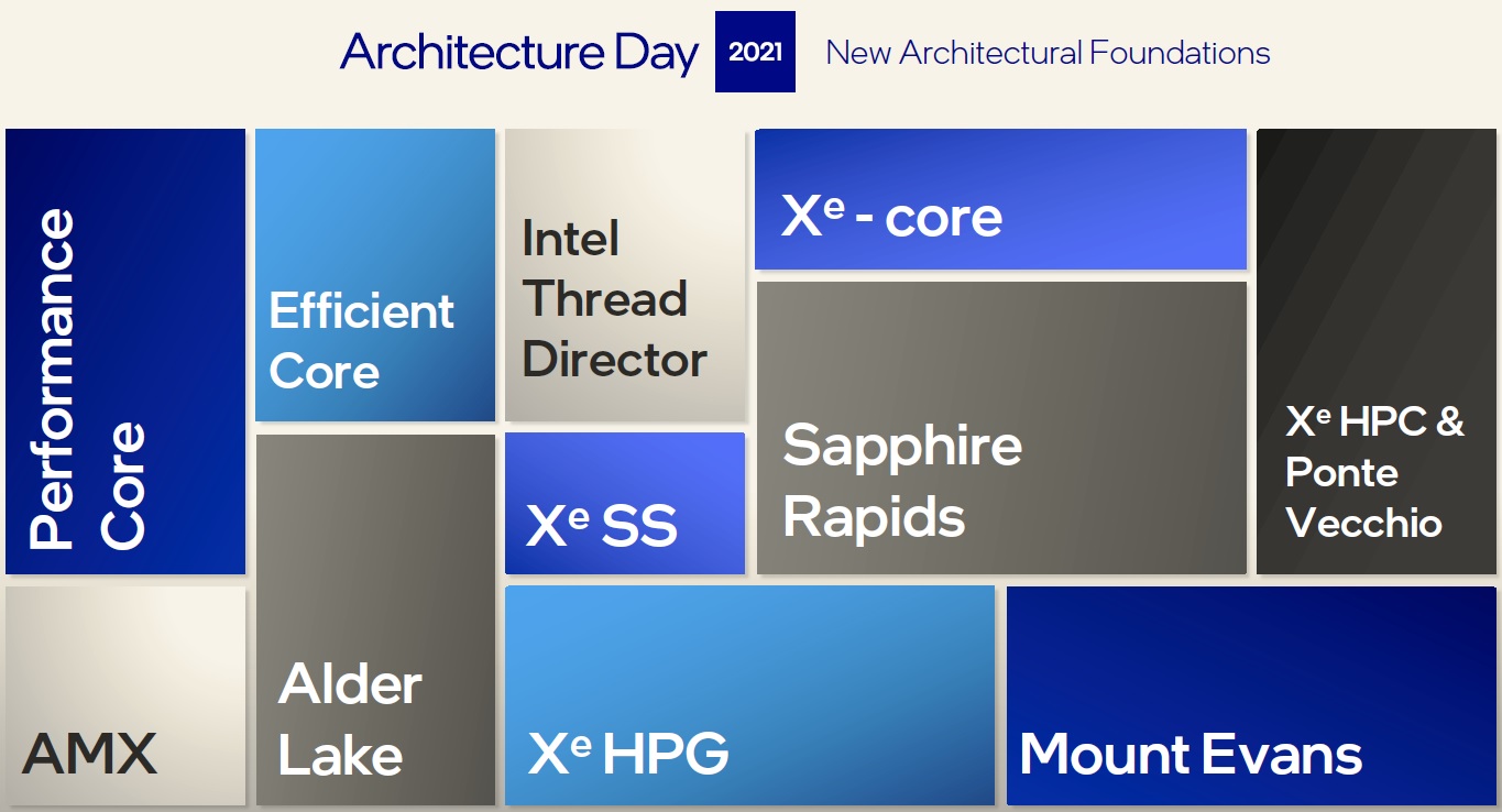
The breadth of topics was vast, encompassing:
- (client and data center) x86 CPUs
- (discrete and integrated) GPUs, from enthusiast and gaming support to high performance AI-centric workloads
- Interface Processing Units (IPUs), to optimize cloud service provider efficiency
- operating system features for managing computing threads in a multi-core complex
- open industry standards for software development application interfaces, focused on the integration of CPU and accelerator devices
This article will attempt to summarize key features of the upcoming CPU releases; a subsequent article will summarize the balance of the presentations.
“Performance” and “Efficient” x86 Cores
Intel introduced two new x86 core implementations – an “efficient” (e-core) and a performance-centric (p-core) offering.
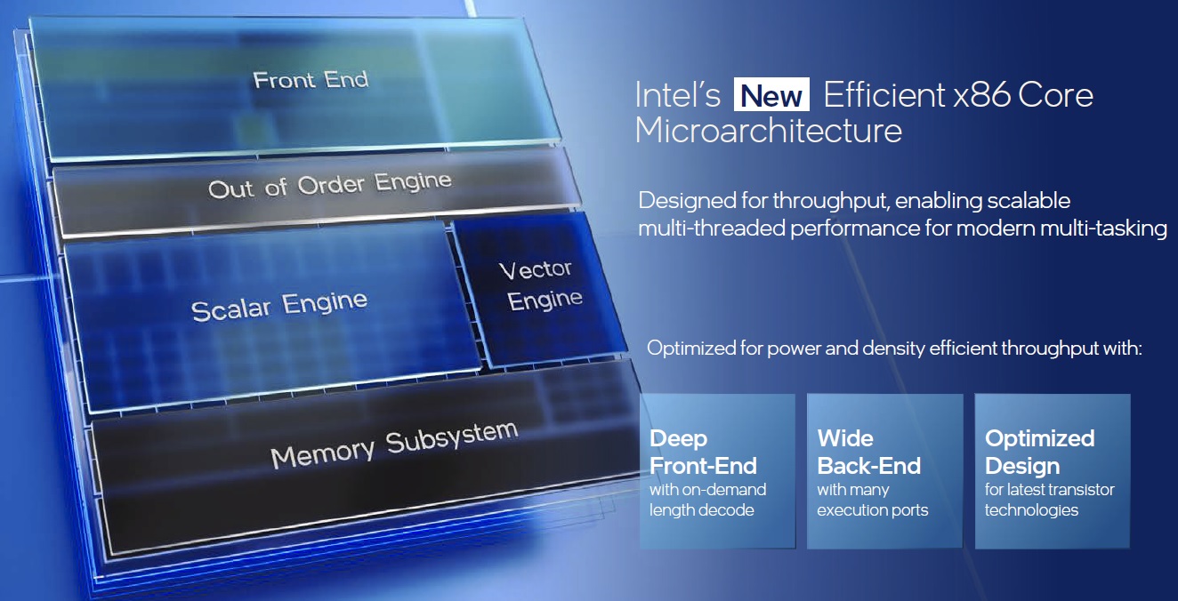
The design considerations for the e-core included:
- cache pre-fetch strategy
- instruction cache size, and data cache size
- L2$ (shared memory) architecture across cores
- branch prediction efficiency, branch target buffer entries
- instruction prefetch bandwidth, instruction retire bandwidth
- x86 complex instruction micro-op decode and reuse strategy
- out-of-order instruction dependency management resources (e.g., allocate/rename register space)
- configuration of various execution units, and address generation load/store units
To maximize the power efficiency of the e-core, a wide (dynamic) supply voltage range is supported.
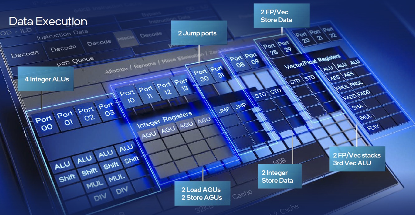
In the figure above, note the units associated with the x86 instructions using vector-based operands, to improve performance of the “dot-product plus accumulate” calculations inherent to deep learning software applications:
- Vector Neural Network Instructions (VNNI, providing int8 calculations)
- Advanced Vector Extensions (AVX-512, for fp16/fp32 calculations)
These instruction extensions accelerate neural network throughput. Active research is underway to determine the optimal data format(s) for neural network inference (with high accuracy), specifically the quantization of larger data types to smaller, more efficient operations – e.g., int4, int8, bfloat16. (The p-core adds another extension to further address machine learning application performance.)
An indication of the e-core performance measures is shown below, with comparisons to the previous generation “Skylake” core architecture – one core executing one thread on the left, and four e-cores running four threads on the right:

Whereas the efficient-core is a highly scalable microarchitecture focusing on multi-core performance per watt in a small footprint, the performance-core focuses on performance, low-latency and multi-threaded performance, with additional AI acceleration.
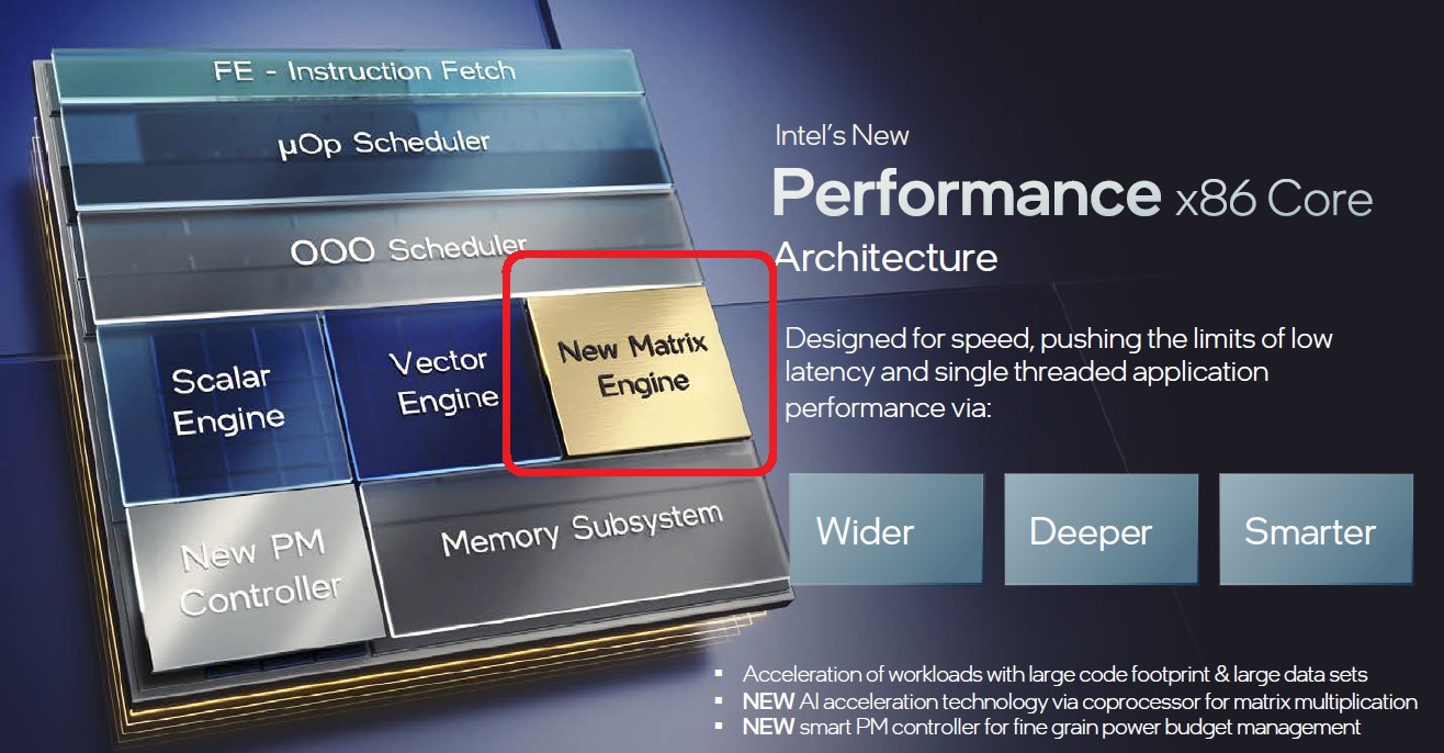
For example, the p-core buffers for OOO instruction reordering management and for data load/store operations are deeper.
As mentioned above, applications are selecting a more diverse set of data formats – the p-core also adds fp16 operation support.
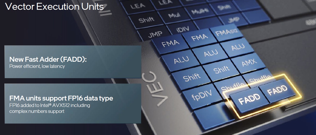
Perhaps the most noteworthy addition to the p-core is the Advanced Matrix Extension instruction set. Whereas vector-based data serve as operands for AVX instructions, the AMX operations work on two-dimensional datasets.

Silicon “tiles” representing 2D register files are integrated with “TMUL” engines providing the matrix operations, as illustrated above.
The addition of AMX functionality is an indication of the diversity of AI workloads. The largest of deep learning neural networks utilize GPU-based hardware for both training and (batch > 1) inference. Yet, there are many AI applications where a relatively shallow network (often with batch = 1) is utilized – and, as mentioned earlier, the use of smaller data types for inference may provide sufficient accuracy, with better power/performance efficiency. It will be very interesting to see how a general purpose CPU with AMX extensions competes with GPUs (or other specialized hardware accelerators) for ML applications.
Thread Director
A key performance optimization in any computer architecture is the scheduling of program execution threads by the operating system onto the processing resources available.
One specific tradeoff is the allocation of a new thread to a core currently executing an existing thread. “Hyperthread-enabled” cores present two logical (virtual) processors to the O/S scheduler. Dual architectural state is provided in the core, with a single execution pipeline. Register, code return stack buffers, etc. are duplicated to support the two threads, at a small cost in silicon area, while subsets of other resources are statically allocated to the threads. Caches are shared. If execution of one thread is stalled, the other is enabled. The cache memory offers some benefit to the two threads, as shared code libraries may be common between threads of the same process.
Another option is to distribute thread execution across separate (symmetric) cores on the CPU until all cores are busy, before invoking hyperthreading.
A combination of p-cores and e-cores in the same CPU (otherwise known as a “big/little” architecture) introduces asymmetry into the O/S scheduler algorithm. The simplest approach would be to distinguish threads based on foreground (performance) and background (efficiency) processes – e.g., using “static” rules for scheduling. For the upcoming CPUs with both p- and e-cores, Intel has integrated additional power/performance monitoring circuitry to provide the O/S scheduler with “hints” on the optimum core assignment – i.e., a runtime-based scheduling approach. An illustration of Intel’s Thread Director is shown below.
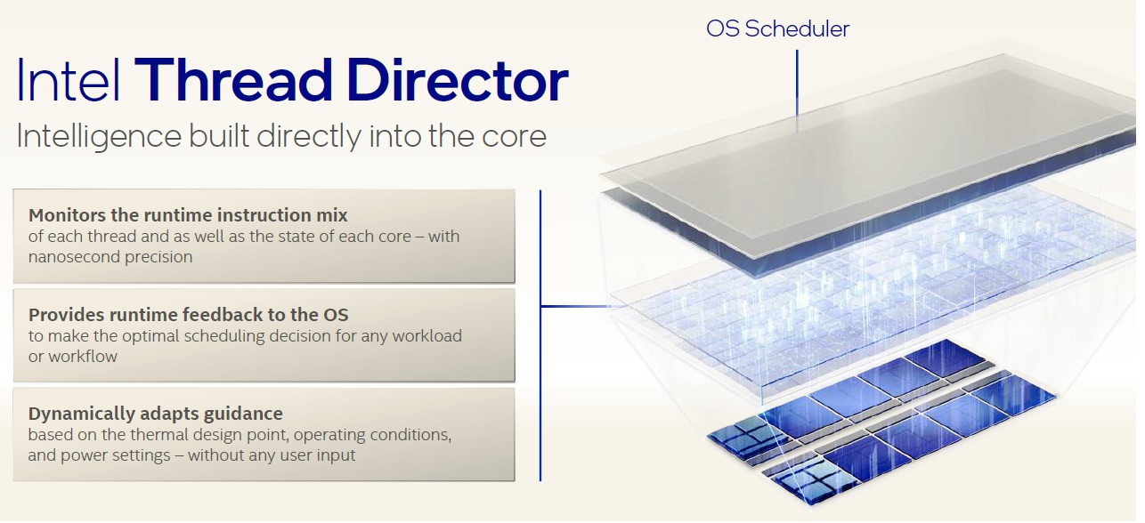
Additionally, based on thread priority, an executing thread could transition between a p-core and e-core. Also, threads may be “parked” or “unparked”.
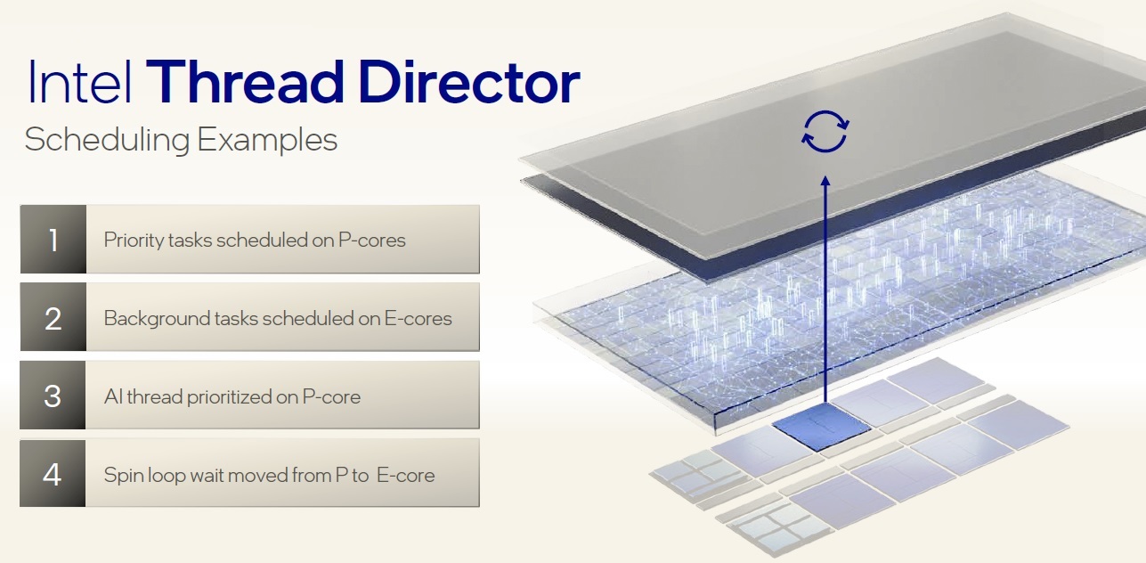
P-cores support hyperthreading, whereas e-cores execute a single thread.
Intel has collaborated with Microsoft to incorporate Thread Director support in the upcoming Windows-11 O/S release. (Windows-10 will still support p- and e-core CPUs, without the real-time telemetry-based scheduler allocation. At the Architecture Day, no mention was made of the status of Thread Director support for other operating systems.)
Alder Lake
The first release of a client CPU with the new p- and c-cores will be Alder Lake, expected to be formally announced at the Intel InnovatiON event in October.
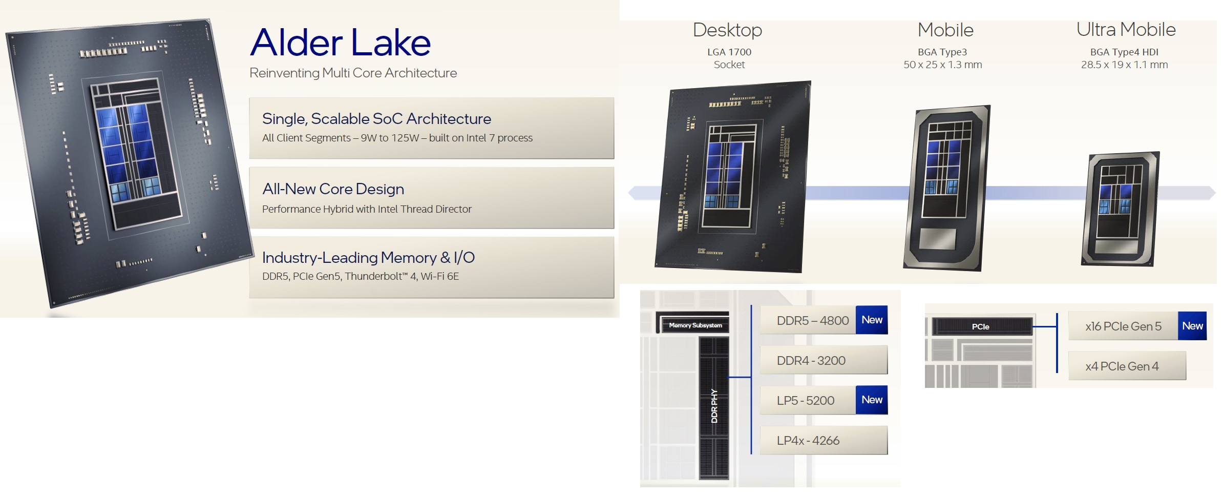
In addition to the new cores, Alder Lake incorporates PCIe Gen 5 and DDR5 memory interfaces. The Alder Lake product family will span a range of target markets, from desktop (125W) to mobile to ultra-mobile (9W), with an integrated GPU core (I7 node).
Sapphire Rapids
The first data center part with the new p-core will be Sapphire Rapids, to be formally announced in 1Q2022 (Intel7 node).
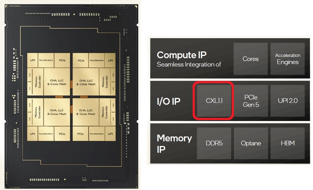
The physical implementation of Sapphire Rapids incorporates “tiles” (also known as “chiplets”), which utilize the unique Intel EMIB bridge silicon for adjacent tile-to-tile dense interconnectivity.
Note that Sapphire Rapids also integrates the Compute Express Link (CXL1.1) industry-standard protocol, to provide a cache-coherent implementation of (heterogeneous) CPU-to-memory, CPU-to-I/O, and CPU-to-device (accelerator) architectures. (For more information, please refer to: www.computeexpresslink.org.)
The memory space is unified across devices – a CPU host manages the cache memory coherency. An I/O device typically utilizes a DMA memory transfer to/from system memory, an un-cached architectural model. With CXL, I/O and accelerator devices enable some/all of their associated memory as part of the unified (cache-coherent) memory space. The electrical and physical interface is based on PCIe. PCIe Gen 5 defines auto-negotiation methods for PCIe and CXL protocols between the host and connected devices.
Another unique feature of Sapphire Rapids is the application of HBM2 memory stacks integrated into the package, as depicted below.
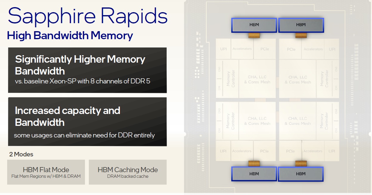
The intent is to provide memory “tiering” – the HBM2 stacks could serve as part of the “flat” memory space, or as caches to external system memory.
Summary
Intel recently described several new products based on p-core and e-core x86 architectural updates, to be shipped in the next few calendar quarters – Alder Lake (client) and Sapphire Rapids (data center). A new Advanced Matrix Extension (AMX) microarchitecture offers a unique opportunity to accelerate ML workloads, fitting a gap in the power/performance envelope between AVX instructions and dedicated GPU/accelerator hardware. The execution of multiples threads on asymmetric cores will benefit from the real-time interaction between the CPU and the (Windows-11) O/S scheduler.
These products also support new PCIe Gen5, DDR5, and the CXL1.1 protocol for unified memory space management across devices.
As mentioned in the Introduction, optimization of systems design is based on tradeoffs in process technology, architecture, and software. The announcements at Intel Architecture Day provide an excellent foundation for current and future product roadmaps, through successive technology generations.
-chipguy
Share this post via:


Comments
There are no comments yet.
You must register or log in to view/post comments.