Digital IC design gets a lot of attention, because all of our modern devices primarily use digital logic, but in reality whenever you have a sensor like a camera, accelerometer, gyroscope or any radio like Bluetooth, WiFi or NFC, then you’re really in the realm of analog, and that’s where mixed-signal IC design comes into play. Siemens EDA has put together an analog/mixed-signal IC design tool flow that looks pretty capable, so I got an update by downloading their latest White Paper on the topic. I did work at Mentor Graphics back in 2003, but a lot has changed over the past 18 years.
Let’s first look at the big picture of the tool flow, split into the Analog (Blue), Digital (Green) and Mixed-Signal (Grey) domains.
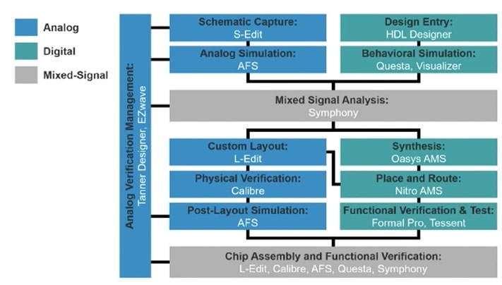
This AMS tool flow supports process node PDKs spanning from 0.5um, all of the way down to 22nm at the following foundries:

Open Access is used as the open reference database for IC design, allowing interoperability between EDA vendors, foundries and fabs. You can even use your favorite data management tool, like: IC Manage, Cliosoft and SubVersion (SVN).
Schematic Capture
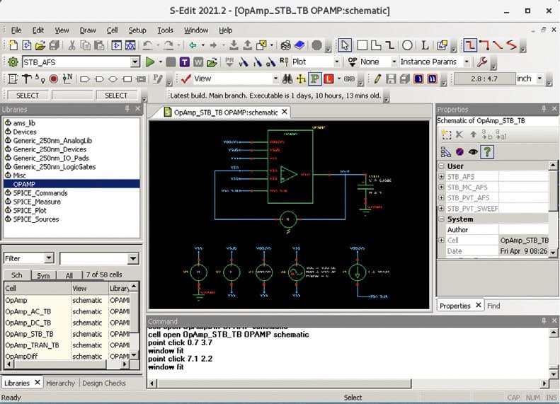
On the front-end, engineers use the S-Edit tool, which came from Tanner EDA in a 2015 acquisition, where you can do transistor-level design, create SPICE netlists, edit Verilog, work with Verilog-A, use Verilog-AMS, or even code VHDL.
Circuit Simulation
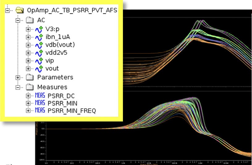
Mentor acquired Berkeley Design Automation back in 2014 and has continued to enhance the Analog FastSPICE (AFS) circuit simulator which is used for analog, RF, mixed-signal and even custom digital circuits. There’s tight integration between S-Edit, AFS and the waveform viewer called EZwave. With Tanner Designer you can do analog verification management, so engineers have a dashboard to see all of their specifications as passing or failing.
Mixed-signal Verification
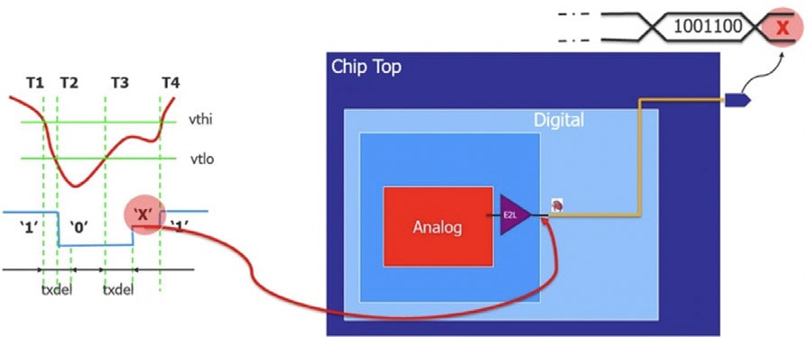
To verify both digital and analog portions of an IC design you need to simulate both realms together, and that’s where the AFS circuit simulator for analog plus Questa simulator for digital come together, and the combination is called Symphony.
Setting up a mixed-signal simulation is done with S-Edit, and each cell instance has a view for the desired abstraction: Schematic, Verilog-A, Verilog, VHDL, SPICE. At the interface between analog and digital ports the Symphony tool automatically inserts a Boundary Element to convert signals properly. Both analog and digital signals are displayed in Symphony, so debugging the AMS interfaces during verification is quicker.
Custom IC Layout
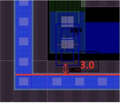
The companion to S-Edit for layout is dubbed L-Edit, and it uses OpenAccess for interoperability, while also supporting PCells for parameterized layout generation. Save time by using Schematic Driven Layout (SDL) along with PCells. Decrease layout verification iterations by using the L-Edit IC Rule-Aware Layout so that you can visually see design rules appear while editing, and it will enforce correct layout.
Digital Implementation
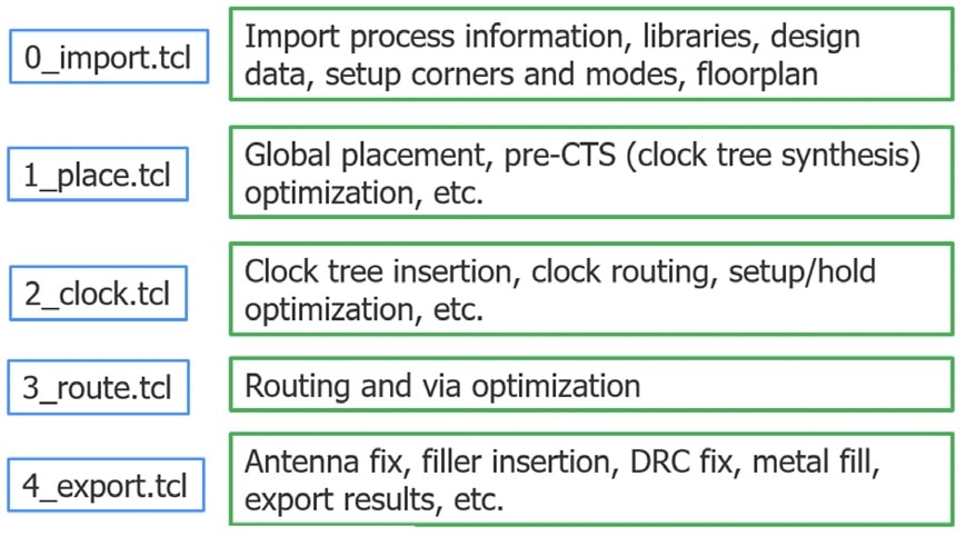
Physical synthesis comes from the Oasys-RTL tool, acquired back in 2013, then the placement and routing task is completed with the Nitro tool. Both tools are launched from the GUI in L-Edit, or you can use command line control if preferred. The complex P&R steps are guided by the Nitro reference flow:
Physical Verification
Siemens EDA is quite famous for it’s leading-edge Calibre tool, and it has several parts called from L-Edit:
- Calibre nmDRC – IC layout design rule checking
- Calibre nmLVS – IC layout versus schematic checking
- Calibre xRC – IC layout extraction for analysis in a circuit simulator like AFS
- Calibre RVE – Results Viewing Environment, for faster layout debug
- Calibre RealTime – interactive DRC checking, prevention approach
Summary
AMS design is harder than just Digital design, so having the right tools and a complete flow of tools will certainly make the task less error-prone, and get done more quickly. Siemens EDA has built up a lot of AMS tool flow experience in the last decades by tightly integrating their own point tools together, while at the same time adopting standards like OpenAccess to ensure interoperability. Whether you adopt an analog on top, or digital on top approach to AMS IC design, both approaches are supported in the Siemens EDA tool flow.
It’s also a healthy sign that so many of the EDA point tool acquisitions have worked out so well over the years in this AMS too flow. Read the complete 10 page White Paper here.
Related Blogs
- RealTime Digital DRC Can Save Time Close to Tapeout
- How About a Faster Fast SPICE? Much Faster!
- Mentor Helps Mythic Implement Analog Approach to AI


Comments
There are no comments yet.
You must register or log in to view/post comments.