You are currently viewing SemiWiki as a guest which gives you limited access to the site. To view blog comments and experience other SemiWiki features you must be a registered member. Registration is fast, simple, and absolutely free so please,
join our community today!
The semiconductor industry is experiencing unprecedented growth in complexity as advanced process nodes, heterogeneous integration, and AI-driven workloads demand increasingly sophisticated chip designs. At the same time, semiconductor companies face rising design costs, increasing engineering workloads, and a shrinking… Read More
By Mark Tawfik
Overview: Protecting ICs from costly ESD and latch-up failures
Electrostatic discharge (ESD) events cost the semiconductor industry an estimated $8 billion annually in lost productivity, warranty claims and product failures [1].
Ensuring the robust protection of integrated circuits (ICs) against various… Read More
By Marko Suominen and Slava Zhuchenya of Siemens Digital Industries Software.
It’s often said that an orchestra without a conductor is just a collection of talented individuals making noise. The conductor’s role is to transform that potential cacophony into a unified, beautiful symphony. The same concept holds… Read More
Calibre is a well-known EDA tool from Siemens that is used for physical verification, but I didn’t really know how AI technology was being used, so I attended a Tuesday session at #62DAC to get up to speed. Priyank Jain, Calibre Product Management presented slides and finished up with a Q&A session.
In the semiconductor world… Read More
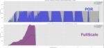
As semiconductor chips shrink and design complexity skyrockets, managing post-tapeout flow (PTOF) jobs has become one of the most compute-intensive tasks in manufacturing. Advanced computational lithography demands an enormous amount of computing power, putting traditional in-house resources to the test. Enter the … Read More
The integration of artificial intelligence (AI) into Electronic Design Automation (EDA) is revolutionizing chip design, addressing the critical shortage of skilled engineers and accelerating the development process. As Jeff Dyck, Senior Director of Engineering at Siemens EDA, explains in a recent DACtv presentation, … Read More
The week before DAC I had the privilege to take a video call with Pradeep Thiagarajan – Product Manager, Simulation, Custom IC Verification at Siemens EDA to get an update on new simulation products. I’ve been following Solido for years now and knew that they were an early adopter of ML for Monte Carlo simulations with SPICE users.… Read More
In the fast-paced world of electronic design automation (EDA) software development, maintaining high code quality while adhering to tight deadlines is a significant challenge. Code coverage, an essential metric in software testing, measures the extent to which a software’s source code is executed in tests. High code… Read More
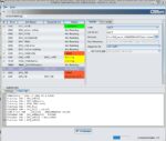
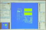
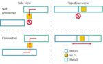
IC designs have physical verification applications like Layout Versus Schematic (LVS) at the transistor-level to ensure that layout and schematics are equivalent, in addition there’s an Electrical Rules Check (ERC) for connections to well regions called a soft check. The connections to all the devices needs to have the most… Read More
Advanced process nodes create challenges for EDA both in handling ever larger designs and increasing design process complexity.
Shift-left design methodologies for design cycle time compression are one response to this. And this has also forced some rethinking about how to build and optimize design tools and flows.
SemiWiki… Read More