Heterogeneous integration (HI) is a general term used to represent the diverse possibilities for die technology incorporated into advanced 2.5D/3D packaging. At the recent International Electron Devices Meeting (IEDM) in San Francisco, a team from Synopsys and IC Knowledge presented data from analyses of future potential HI implementations.[1]
This article briefly summarizes the highlights of their paper, with an emphasis on the rather startling HI cost analysis.
HI Interconnects
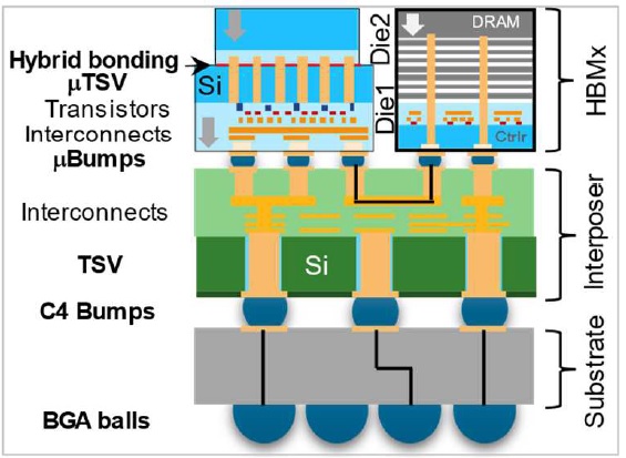
The nomenclature for advanced HI packaging is illustrated in the figure below.

A complex HI package could incorporate:
- 3D (thinned die) high-bandwidth memory DRAM stacks
- 3D stacked die
- a 2.5D interposer, with redistribution layers (RDL) for signal interconnects between die and the package substrate
- a hierarchy of attach technologies:
- C4 bumps (~110-150um pitch)
- microbumps for die-to-interposer attach (~40-55um pitch)
- hybrid bonded (bumpless) attach, for 3D stacked die, in either a face-to-face or face-to-back orientation
- through silicon vias (TSVs) in the interposer between the bumps and RDL layers
- micro-TSVs through the silicon in the 3D die stack (~10um pitch)
There is also the potential to replace the silicon interposer with smaller silicon “bridges” between die edges in the 2.5D configuration, maintaining the high interconnect density while reducing cost (not shown in the figure above). The tradeoff with the use of bridges embedded in an organic substrate versus an interposer is the redistribution interconnect density is reduced considerably.
HI Interconnect Electrical Analysis
A key requirement of any heterogeneous integration system is the available bus bandwidth for data communication between die.
An electrical design consideration is whether the interconnect characteristics between die (on the interposer or bridge) will support wide parallel bus signaling at lower clock rates to achieve the requisite throughput, or whether a more sophisticated (and more power-hungry) high-speed serial interface design is required.
A physical and electrical analysis of the interconnects includes estimates for:
- interconnect density
- package wire length
- signal latency from Tx-to-Rx
- losses (signal fidelity at the receiver circuitry)
- bit error rate (past the receiver)
- power/bit
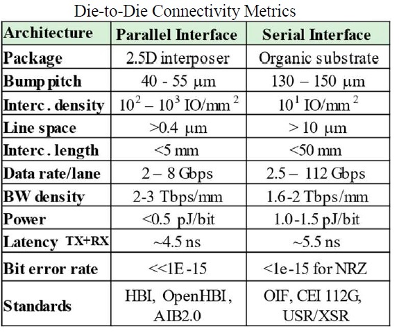
The interconnect density of interposer (or bridge) RDL wires has led to the development of parallel bus electrical standards for die-to-die communications in advanced 2.5D packages, such as AIB [2] and OpenHBI [3].
Synopsys commented that the circuit challenges for the PHY IP for a parallel HBI interface (@ 4Gbps) are “far less demanding” than for a SerDes operating at a much higher datarate. This interface is optimal for interconnect lengths on the order of ~5mm. The table below from the presentation highlights the serial versus parallel interface tradeoffs.

For die-to-die interconnect lengths afforded by 3D hybrid bonding (~1um), direct buffered signaling is viable – no PHY required.
PDN for Heterogeneous Integration
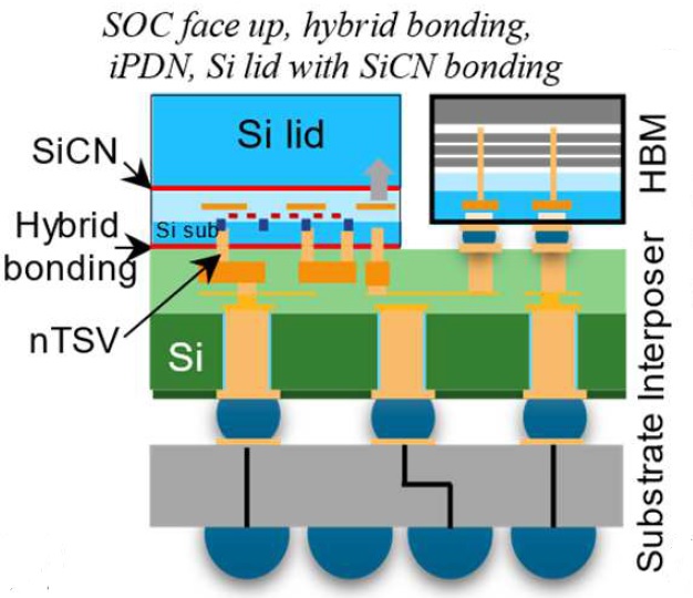
Another design consideration is how to provide the global power distribution network (PDN) to the HI configuration. The figure below illustrates a unique 2.5D die plus HBM topology proposed by the Synopsys team, where the PDN is fabricated directly on the interposer.

The interposer with PDN is hybrid-bonded to the backside of an ultra-thinned die, with “nano-TSVs” at 3um pitch connecting to buried power rails (BPRs) embedded locally with the logic circuitry. A silicon lid “carrier” is bonded to the top side of the die to support the die ultra-thinning process. This configuration offers simplified PDN processing, improved I*R drop on the VDD/GND supplies, and frees up BEOL routing tracks on the die for improved circuit density.
(Foundries are also working on single-die backside PDN fabrication process capability. This proposal leverages the presence of the 2.5D interposer for HI configurations.)
HI Cost Analysis
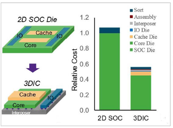
An enlightening part of the Synopsys presentation related to an analysis of the relative costs of a monolithic versus disaggregated HI implementation. The team worked with IC Knowledge, LLC on the financial forecast models.[4] (Note that the configuration below uses 2nm process technology estimates.)
The parameters used for this comparative analysis were:
SoC: 2nm process note, gate-all-around devices, 17-layer metal (17LM), 600mm**2 die size, with 65% logic, 20% L3 SRAM, 10% I/O
HI implementation: Core die in the original 17-layer metal 2nm process, L3 SRAM die in 4-layer metal 2nm process hybrid bonded to base die, separate I/O die in 7-metal layer 90nm process on 2.5D interposer
The figure below illustrates the results of the analysis – a 48% cost reduction!

The cost benefits accrue from:
- higher die yields
- no need for 17LM fabrication for the non-logic functions
- 4LM in the 2nm process for the L3
- 7LM in a 90nm process for the I/O
These cost reductions more than compensate for the additional expense related to:
- die sort
- 6LM silicon interposer with TSVs
- HI assembly, test
Summary
Advanced packaging technology has enabled heterogeneous integration of disaggregated functionality where different process technologies (and BEOL options) are available for the individual die. The analysis by Synopsys and IC Knowledge indicates the cost advantages of a 3D + 2.5D HI configuration can be substantial.
Additionally, this packaging technology offers tradeoffs in the choice of serial versus parallel bus implementations. For the high interconnect density and short length of 2.5D signaling, wide parallel buses offer the requisite data bandwidth with simpler circuitry and lower pJ/bit power dissipation.
The Synopsys IEDM presentation also illustrated an alternative for the PDN, utilizing the interposer with ultra-thin die and nano-TSV connections.
-chipguy
References
[1] Lin, X.-W., et al., “Heterogeneous Integration Enabled by State-of-the-Art 3DIC and CMOS Technologies: Design, Cost, and Modeling”, IEDM 2021, paper 3.4.
[2] https://github.com/chipsalliance/AIB-specification
[3] https://www.synopsys.com/designware-ip/technical-bulletin/openhbi-die-to-die.html
[4] https://www.icknowledge.com/
All images in this article are copyrighted by the IEEE.
Also Read:
Delivering Systemic Innovation to Power the Era of SysMoore
Creative Applications of Formal at Intel
Synopsys Expands into Silicon Lifecycle Management
Share this post via:


Comments
5 Replies to “Heterogeneous Integration – A Cost Analysis”
You must register or log in to view/post comments.