The further scaling of interconnect and via lithography for advanced nodes is challenged by the requirement to provide a process window that supports post-patterning critical dimension variations and mask overlay tolerances. At the recent international Electron Devices Meeting (IEDM) in San Francisco, TSMC presented a research update on their process development activities to realize a “self-aligned via” (SAV) for upcoming nodes, with an interconnect + via flow that provides improved manufacturability.[1] This article summarizes the highlights of their presentation.
Introduction
The manufacturability of vias needs to address multiple litho, electrical, and reliability measures:
- tolerance to overlay variation (aka, “edge placement error”, or EPE)
- consistency of via resistance
- robustness of via-to-adjacent metal dielectric properties
- leakage current
- maximum applied voltage before breakdown (Vbd)
- dielectric reliability, measured as time-dependent dielectric breakdown (TDDB)
and, of course,
- exceptional yield
(Note that these issues are most severe for the scaling of lower level metals and vias, denoted as “Mx” in the figures in this article.)
The overlay positioning between a via and an adjacent metal line impacts the dielectric breakdown – both Vbd and TDDB. The figure below illustrates the overlay versus dielectric breakdown issue of a conventional via, for a representative EPE.

A “self-aligned” via (with a unique dielectric to an adjacent metal line) would provide greater process latitude to address the challenges listed above.
TSMC SAV Process
There are two key steps to the TSMC SAV process flow – the deposition of a “blocking layer” on metal lines and the selective deposition of dielectric-on-dielectric.
- self-assembled monolayer (SAM) deposition on metal
A unique process chemistry step deposits a monolayer of a blocking material on an exposed metal surface. This process is based on the affinity of organic chemical chains suspended in a solution to the metal. The molecular chains are adsorbed on the metal surface, and self-assemble into an organized domain. As the molecules adsorb over time, they will nucleate into groups and grow until the metal surface is covered with a monolayer. (The monolayer packs tightly due to the van der Waals forces, the weak net attractive electric force between neutral organic solids.)
This SAM monolayer will serve as a blocking material. Its composition needs to withstand the thermal exposure of the next step – the selective dielectric deposition on oxide.
- selective dielectric-on-dielectric (DoD) deposition
Advanced nodes have leveraged atomic layer deposition (ALD) steps for several generations. A gas phase “pre-cursor” is introduced into the process chamber. Due to chemisorption, a unique pre-cursor monolayer is deposited on the wafer surface. The pre-cursor adheres to the surface, but not to itself – no successive pre-cursor layers are deposited. The chamber is then purged of the excess pre-cursor, and a co-reagent is subsequently introduced. The chemical reaction results in a final monolayer of the desired reaction product that remains on the surface, while the excess co-reagent and reaction by-products are pumped out. The cycle can be repeated to deposit multiple “atomic” layers. ALD has been widely adopted for the deposition of metal and thin-oxide dielectric materials. A key advantage of current ALD processes is they operate uniformly and conformally on the exposed wafer surface.
An active area of research is to provide selective area atomic layer deposition, where the pre-cursor only adheres to a specific material surface. The goal is the pre-cursor adsorption is suppressed on specific areas – in this case, the SAM molecules on the metal.
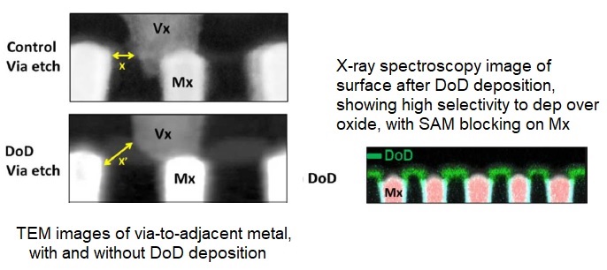
TSMC explored a selective deposition chemical process, for dielectric-on-dielectric layer buildup. The images in the figure below depict the process flow to raise a dielectric layer above the existing surface oxide.

The SAM blocking layer precludes the selective deposition on the exposed dielectric. As mentioned earlier, the blocking layer must withstand exposure to the elevated temperature of the dielectric-on-dielectric selective deposition. TSMC indicated that higher DoD process temperatures improve the etch selectivity of the dielectric pedestal to the surrounding low-K inter-level dielectric for the via, to be discussed next.
The image labeled “DoD” in the figure above illustrates the wafer after dielectric-on-dielectric deposition and after removal of the SAM blocking material over the wafer, prior to the addition of the low-K dielectric.
The image on the right shows the final via connection, after low-K dielectric dep/etch and via patterning. The added DoD material serves as a suitable “etch stop”, due to the lower etch rate compared to the low-K material. This image illustrates the via-to-adjacent metal dielectric, in the presence of a significant overlay shift.
The figure below illustrates how the added dielectric-on-dielectric layer improves via robustness. The “control” transmission electron microscopy image (without the DoD) shows excessive via etch of the original dielectric, with little isolation to the adjacent Mx line – not particularly tolerant of overlay error. The DoD TEM image shows vastly improved isolation.

Experimental Electrical and Reliability Data for the SAV Process
The various figures below show the experimental data from the TSMC SAV process development team. The Control data reflects the standard via patterning process without the selective DoD layer deposition.
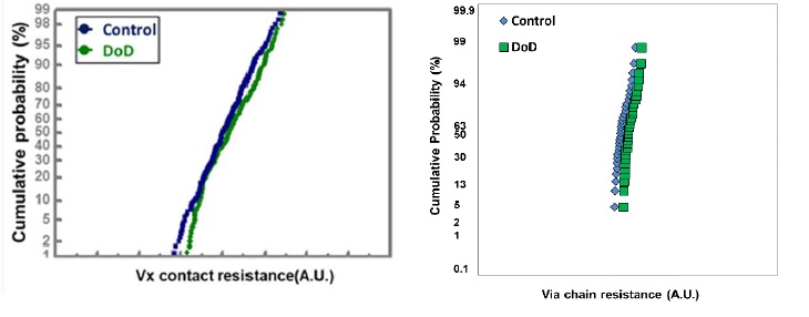
- via resistance

Both single via and via chain (yield assessment) resistance values show no difference between the control and DoD processes.
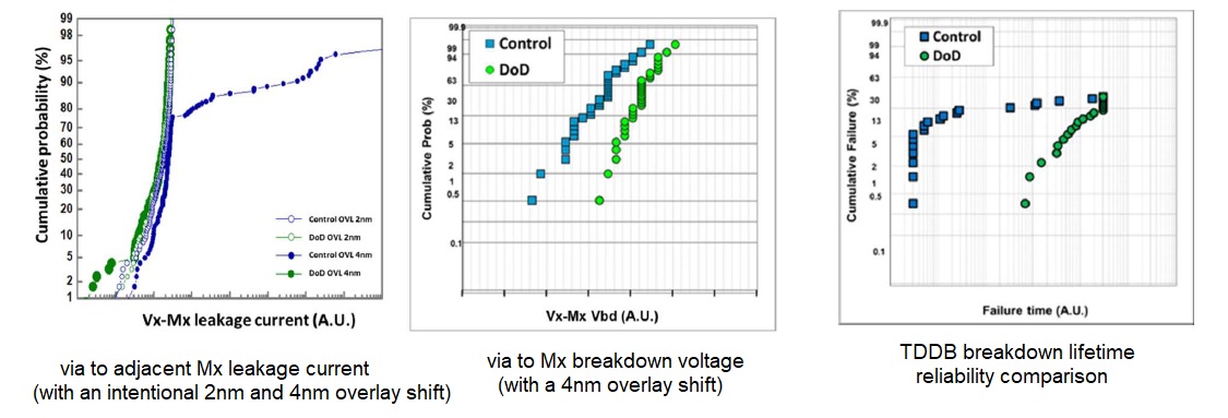
- via-to-adjacent Mx reliability (leakage current, Vbd, TDDB)

To assess the process window, the TSMC team evaluated the leakage current and Vbd with an intentional via-to-Mx overlay shift. Note that the control process would not support a 4nm overlay tolerance.
To ensure the additional DoD process steps did not adversely impact the characteristics of the existing Mx metal, TSMC shared evaluation data of metal lines with and without the DoD process. The graphs below show there was no impact to metal line resistance or TDDB/electromigration reliability.

Summary
Continued interconnect scaling below the 3nm node will necessitate unique process development research to maintain electrical and reliability specs in the presence of (up to 4nm) overlay error. The need for low-K interlevel dielectrics is a given – yet, the via etch in these materials is not especially tolerant of EPE.
TSMC has demonstrated a potential process flow for a “self-aligned via” with an additional DoD material. The etch rate differential of the DoD results in more robust via-to-adjacent metal reliability. This process flow utilizes two unique steps – the SAM of a blocking material on metal surfaces, and the selective ALD of a dielectric-on-dielectric.
Hopefully, selective ALD flows will transition soon from R&D to production fabrication – the potential impact of this chemistry for advanced node scaling is great.
-chipguy
References
[1] Chen, H.-P., et al, “Fully Self-Aligned via Integration for Interconnect Scaling Beyond 3nm Node”, IEDM 2021, paper 22-1.
Note: All images are copyright of the IEEE.
Share this post via:


Comments
One Reply to “Self-Aligned Via Process Development for Beyond the 3nm Node”
You must register or log in to view/post comments.