You are currently viewing SemiWiki as a guest which gives you limited access to the site. To view blog comments and experience other SemiWiki features you must be a registered member. Registration is fast, simple, and absolutely free so please,
join our community today!
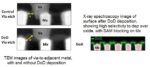
The further scaling of interconnect and via lithography for advanced nodes is challenged by the requirement to provide a process window that supports post-patterning critical dimension variations and mask overlay tolerances. At the recent international Electron Devices Meeting (IEDM) in San Francisco, TSMC presented … Read More
Since the beginning of the semiconductor industry, improving the rate of yield learning has been a critical factor in the success silicon manufacturing. Each fab has dedicated yield teams that look at the yield of wafers manufactured the previous day and attempt to find the root cause of any unexpected “excursions.” In earlier… Read More