Since the beginning of the semiconductor industry, improving the rate of yield learning has been a critical factor in the success silicon manufacturing. Each fab has dedicated yield teams that look at the yield of wafers manufactured the previous day and attempt to find the root cause of any unexpected “excursions.” In earlier times it was assumed that as long as a design passed design rule checking (DRC) that it would have acceptable yields when manufactured, but that is no longer the case. Now at advanced nodes there is sufficient manufacturing sensitivity to specific design features that it is increasingly common that design-related yield issues can appear even for designs that have passed all DRC checks. Some of the design induced issues include line edge roughness, dishing from chemical mechanical polishing (CMP), and pull back of drawn features (e.g. metal overlap over a VIA). In order to prevent these effects the design must be made more robust by employing Design for Manufacturing (DFM) strategies such as via doubling, litho hotspot detection, and Optical Proximity Correction (OPC).

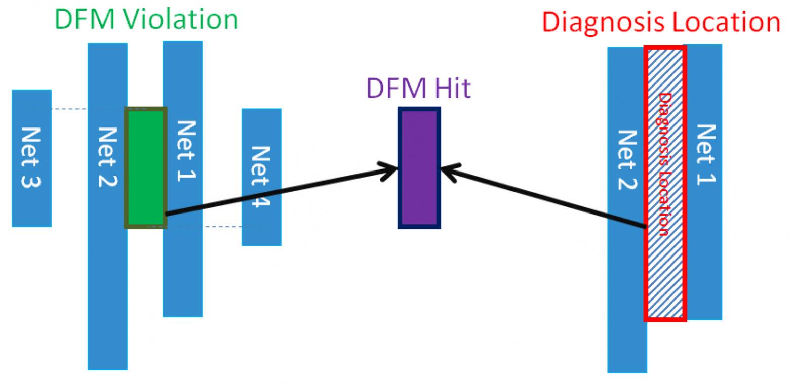
The green polygon (left) is a critical feature location in the design as determined by DFM analysis. The red rectangle (right) is the diagnosed defect location for a bridge between two nets on one device failing manufacturing test. The purple box (center) is the intersection of critical feature analysis (CFA) and test failure diagnosis.
Layout structures that are most susceptible to manufacturing process variability are called critical features. Critical features are believed to be increasing in number, but it is difficult to justify expensive test chip experiments to quantify critical feature impact. Historically yield engineers have identified systematic critical features by identifying higher than expected yield loss in silicon, submitting selected die to physical failure analysis (PFA) and obtaining at least two similar results, and then bringing in a panel of experts from across the company to hypothesize the true root cause based on the failure analysis results. Finally, experiments are devised to prove or disprove the hypothesis, for example, split lots or short loop experiments. In general this is an effective methodology, but very slow and expensive because of the reliance on PFA and multiple subject matter experts (SMEs).
An alternate approach, which creates actionable data to facilitate yield learning at the fabless-foundry interface, is currently being evaluated by Mentor Graphics and GLOBALFOUNDRIES. The focus of this method is to provide the most precise description of the critical feature in terms of the immediately surrounding geometry. This is determined by evaluating several similar but different critical feature hypotheses in order to find the best fit for a population of die that have failed production testing. This means that every design essentially becomes a test chip that can be used to improve yield leaning, and ultimately the design and manufacturing process. The key to making this approach workable is to capture the right data from chip production testing, and to provide powerful statistical analysis tools to help engineers identify and organize correlations in the data that point to the critical features.
A description of this methodology is provided in a paper authored by Mentor and GLOBALFOUNDRIES, which is available on Mentor’s foundry solutions web site. (See “GLOBALFOUNDRIES and Mentor Develop Methods to Identify Critical Features in IC Designs.”)
Share this post via:


Is Intel About to Take Flight?