You are currently viewing SemiWiki as a guest which gives you limited access to the site. To view blog comments and experience other SemiWiki features you must be a registered member. Registration is fast, simple, and absolutely free so please,
join our community today!
Daniel is joined by Sagar Saxena, Senior Product Engineer at Siemens EDA specializing in computational lithography, optical proximity correction (OPC), and advanced patterning solutions for leading-edge semiconductor manufacturing. Sagar has led the development and deployment of advanced OPC technologies, including… Read More
As semiconductor manufacturing pushes toward advanced nodes with tighter feature sizes, the optical proximity correction (OPC) workflow is adopting curvilinear masks to achieve the larger process windows that traditional Manhattan geometries cannot deliver.
Traditional Manhattan masks constrain shapes to vertical … Read More
Masks have always been an essential part of the lithography process in the semiconductor industry. With the smallest printed features already being subwavelength for both DUV and EUV cases at the bleeding edge, mask patterns play a more crucial role than ever. Moreover, in the case of EUV lithography, throughput is a concern, … Read More
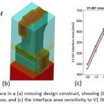
Physical verification is an important and necessary step in the process to tapeout an IC design, and the foundries define sign-off qualification steps for:
- Physical validation
- Circuit validation
- Reliability verification
This sounds quite reasonable until you actually go through the steps only to discover that some of the … Read More
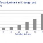
Technology trends make the concerns with electronic noise a primary constraint that impacts many mainstream products, driving the need for “Design-for-Noise” practices. That is, scaling, and the associated reduction in the device operating voltage and current, in effect magnifies the relative importance of non-scalable… Read More
As feature sizes have shrunk, the semiconductor industry has moved from simple, single-exposure lithography solutions to increasingly complex resolution-enhancement techniques and multi-patterning. Where the design on a mask once matched the image that would be produced on the wafer, today the mask and resulting image … Read More
The ability to extend photolithography utilizing 193i light sources to current process nodes is truly the key technical achievement that has enabled Moore’s Law to continue. The interplay between the exposure equipment, the materials – especially, resists and related coatings – and the fundamental principles… Read More
For any semiconductor technology node to be adopted in actual semiconductor designs, the very first step is to have a Process Design Kit (PDK) developed for that particular technology node and qualified through several design tools used in the design flow. The development of PDK has not been easy; it’s a tedious, time consuming,… Read More
The Matrix, your ultimate OPCby Beth Martin on 05-06-2014 at 12:47 pmCategories: EDA
One of the many consequences of shrinking process nodes is that traditional OPC can no longer achieve good pattern fidelity with reasonable turn-around-time. But there is a solution; we made it ourselves and call it matrix OPC.
First, let’s explore the problems with traditional optical proximity correction (OPC) when applied… Read More
One SPIE session not to missby Beth Martin on 02-19-2014 at 4:19 pmCategories: EDA, Siemens EDA
The time is nigh for another meeting of the practitioners of the lithographic arts, dark and otherwise, at the SPIE Advanced Lithography symposium.
I love this conference for the engagement you see, both in the sessions and in the hallways. People actually meet and talk and argue. There’s always interesting gossip, exciting technologies,… Read More