
Masks have always been an essential part of the lithography process in the semiconductor industry. With the smallest printed features already being subwavelength for both DUV and EUV cases at the bleeding edge, mask patterns play a more crucial role than ever. Moreover, in the case of EUV lithography, throughput is a concern, so the efficiency of projecting light from the mask to the wafer needs to be maximized.
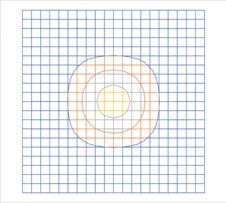
Conventional Manhattan features (named after the Manhattan street blocks or the lit building windows in the evening) are known for their sharp corners, which naturally scatter light outside the numerical aperture of the optical system. In order to minimize such scattering, one may to turn to Inverse Lithography Technology (ILT), which will allow curvilinear feature edges on the mask to replace sharp corners. To give the simplest example where this may be useful, consider the target optical image (or aerial image) at the wafer in Figure 1, which is expected from a dense contact array with quadrupole or QUASAR illumination, resulting in a 4-beam interference pattern.

Figure 1. A dense contact image from quadrupole or QUASAR illumination, resulting in a four-beam interference pattern.
Four interfering beams cannot produce sharp corners at the wafer, but a somewhat rounded corner (derived from sinusoidal terms). A sharp feature corner on the mask would produce the same roundness, but with less light arriving at the wafer; a good portion of the light has been scattered out. A more efficient transfer of light to the wafer can be achieved if the mask feature has a curvilinear edge with the same roundness, as in Figure 2.

Figure 2. Mask feature showing curvilinear edge similar to the image at the wafer shown in Figure 1. The edge roundness ideally should be the same.
The amount of light scattered out can be minimized to 0 ideally with curvilinear edges. Yet despite the advantage of curvilinear edges, it has been difficult to make masks with these features, as curvilinear edges require more mask writer information to be stored compared to Manhattan features, reducing the system throughput from the extra processing time. The data volume required to represent curvilinear shapes can be an order of magnitude more than the corresponding Manhattan shapes. Multi-beam mask writers, which have only recently become available, compensate the loss of throughput.
Mask synthesis (designing the features on the mask) and mask data prep (converting the said features to the data directly used by the mask writer) also need to be updated to accommodate curvilinear features. Synopsys recently described the results of its curvilinear upgrade. Two highlighted features for mask synthesis are Machine Learning and Parametric Curve OPC. Machine learning is used to train a continuous deep learning model on selected clips. Parametric Curve OPC represents curvilinear layer output as a sequence of parametric curve shapes, in order to minimize data volume. Mask data prep comprises four parts: Mask Error Correction (MEC), Pattern Matching, Mask Rule Check (MRC), and Fracture. MEC is supposed to compensate errors from the mask writing process, such as electron scattering from the EUV multilayer. Pattern matching operations search for matching shapes and becomes more complicated without restrictions to only 90-deg and 45-deg edges. Likewise, MRC needs new rules to detect violations involving curved shapes. Finally, fracture needs to not only preserve curved edges but also support multi-beam mask writers.
Synopsys includes all these features in its full-chip curvilinear data processing system, which are fully described from the white paper here: https://www.synopsys.com/silicon/resources/whitepapers/curvilinear_mask_patterning.html.
Also Read:
Chiplet Q&A with Henry Sheng of Synopsys
Synopsys Accelerates First-Pass Silicon Success for Banias Labs’ Networking SoC
Multi-Die Systems: The Biggest Disruption in Computing for Years
Share this post via:


Comments
There are no comments yet.
You must register or log in to view/post comments.